May 24, 2018
Rare element to provide better material for high-speed electronics
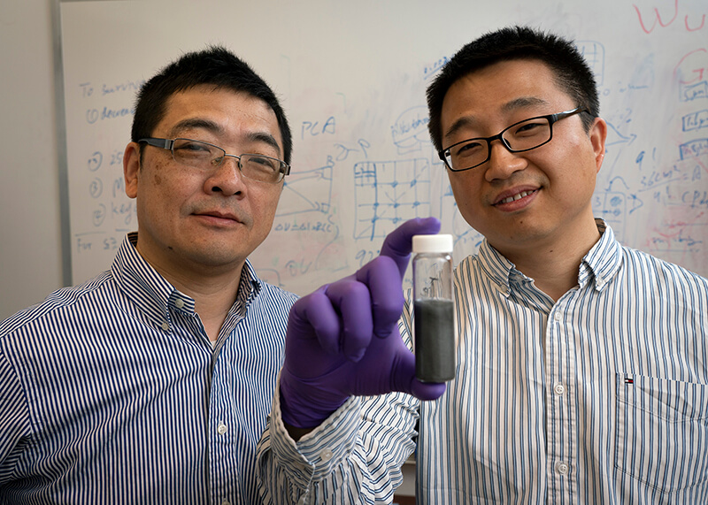
 Purdue researchers Wenzhuo Wu and Peide Ye recently discovered tellurene, a two-dimensional material they manufactured in a solution, that has what it takes to make high-speed electronics faster. (Purdue University image/Vincent Walter)
Download image
WEST LAFAYETTE, Ind. — Purdue researchers have discovered a new two-dimensional material, derived from the rare element tellurium, to make transistors that carry a current better throughout a computer chip.
The discovery adds to a list of extremely thin, two-dimensional materials that engineers have tried to use for improving the operation speed of a chip’s transistors, which then allows information to be processed faster in electronic devices, such as phones and computers, and defense technologies like infrared sensors.
Other two-dimensional materials, such as graphene, black phosphorus and silicene, have lacked either stability at room temperature or the feasible production approaches required to nanomanufacture effective transistors for higher speed devices.
“All transistors need to send a large current, which translates to high-speed electronics,” said Peide Ye, Purdue’s Richard J. and Mary Jo Schwartz Professor of Electrical and Computer Engineering. “One-dimensional wires that currently make up transistors have very small cross sections. But a two-dimensional material, acting like a sheet, can send a current over a wider surface area.”
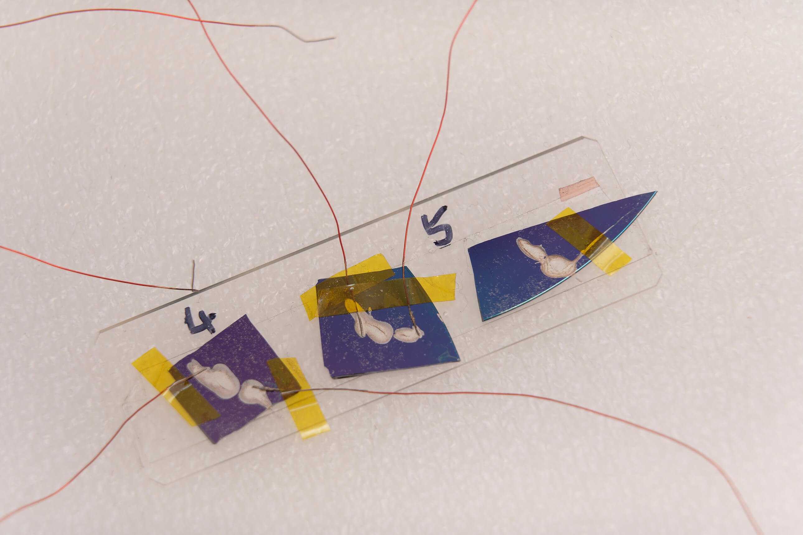
 A small quantity of two-dimensional tellurene, derived from the rare element tellurium, can make computer chip transistors both more scalable and efficient. (Purdue University image/Vincent Walter)
Download image
Tellurene, a two-dimensional film researchers found in the element tellurium, achieves a stable, sheet-like transistor structure with faster-moving “carriers” – meaning electrons and the holes they leave in their place. Despite tellurium’s rarity, the pros of tellurene would make transistors made from two-dimensional materials easier to produce on a larger scale. The researchers detail their findings in Nature Electronics.
“Even though tellurium is not abundant on the Earth’s crust, we only need a little bit to be synthesized through a solution method. And within the same batch, we have a very high production yield of two-dimensional tellurene materials,” said Wenzhuo Wu, assistant professor in Purdue’s School of Industrial Engineering. “You simply scale up the container that holds the solution, so productivity is high.”
Since electronics are typically in use at room temperature, naturally stable tellurene transistors at this temperature are more practical and cost-effective than other two-dimensional materials that have required a vacuum chamber or low operation temperature to achieve similar stability and performance.
The larger crystal flakes of tellurene also mean less barriers between flakes to electron movement – an issue with the more numerous, smaller flakes of other two-dimensional materials.
“High carrier mobility at room temperature means more practical applications,” Ye said. Faster-moving electrons and holes then lead to higher currents across a chip.
The researchers anticipate that because tellurene can grow on its own without the help of any other substance, the material could possibly find use in other applications beyond computer chip transistors, such as flexible printed devices that convert mechanical vibrations or heat to electricity.
“Tellurene is a multifunctional material, and Purdue is the birthplace for this new material,” Wu said. “In our opinion, this is much closer to the scalable production of two-dimensional materials with controlled properties for practical technologies.”
Wu and Ye’s work was supported by Purdue’s College of Engineering and School of Industrial Engineering, the National Science Foundation, Oak Ridge Associated Universities, the Air Force Office of Scientific Research, the Army Research Office and the Semiconductor Research Corporation. Collaborating paper authors received various funding from fellowships and grants.
Writer: Kayla Wiles, 765-494-2432, wiles5@purdue.edu
Sources: Wenzhuo Wu, 765-494-7082, wenzhuowu@purdue.edu, https://engineering.purdue.edu/wugroup
Peide Ye, 765-494-7611, yep@purdue.edu, https://engineering.purdue.edu/~yep
Note to Journalists: For a full-text copy of the paper, please contact Kayla Wiles, Purdue News Service, at wiles5@purdue.edu.
ABSTRACT
Field-effect transistors made from solution-grown two-dimensional tellurene
Yixiu Wang1, Gang Qiu2, Ruoxing Wang1, Shouyuan Huang1, Qingxiao Wang2, Yuanyue Liu3,4, Yuchen Du1, William A. Goddard III3, Moon J. Kim1, Xianfan Xu1, Peide D. Ye1, Wenzhuo Wu1
1Purdue University, West Lafayette, IN, USA
2University of Texas at Dallas, Richardson, TX, USA
3California Institute of Technology, Pasadena, CA, USA
4University of Texas at Austin, Austin, TX, USA
doi: 10.1038/s41928-018-0058-4
The reliable production of two-dimensional (2D) crystals is essential for the development of new technologies based on 2D materials. However, current synthesis methods suffer from a variety of drawbacks, including limitations in crystal size and stability. Here, we report the fabrication of large-area, high-quality 2D tellurium (tellurene) using a substrate-free solution process. Our approach can create crystals with process-tunable thickness, from a monolayer to tens of nanometres, and with lateral sizes of up to 100 µm. The chiral-chain van der Waals structure of tellurene gives rise to strong in-plane anisotropic properties and large thickness-dependent shifts in Raman vibrational modes, which is not observed in other 2D layered materials. We also fabricate tellurene field-effect transistors, which exhibit air-stable performance at room temperature for over two months, on/off ratios on the order of 106, and field-effect mobilities of about 700 cm2 V−1 s−1. Furthermore, by scaling down the channel length and integrating with high-k dielectrics, transistors with a significant on-state current density of 1 A mm−1 are demonstrated.

