
April 29, 2020
Engineers make a promising material stable enough for use in solar cells
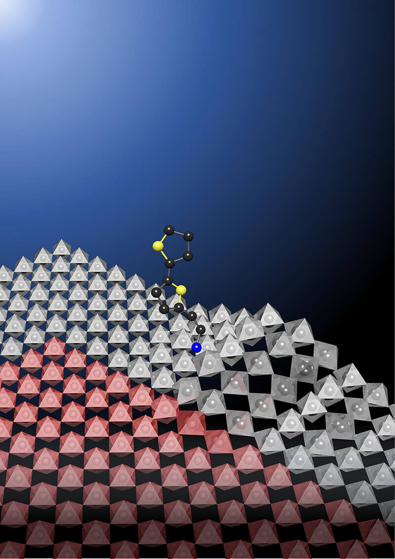 Just adding a bulky molecule to the surface of a perovskite might finally make the material stable enough for incorporating into solar panels. (Purdue University illustration/Enzheng Shi)
Download image
Just adding a bulky molecule to the surface of a perovskite might finally make the material stable enough for incorporating into solar panels. (Purdue University illustration/Enzheng Shi)
Download image
Simple change to perovskite surface removes barrier to its functionality
WEST LAFAYETTE, Ind. — Soft and flexible materials called halide perovskites could make solar cells more efficient at significantly less cost, but they’re too unstable to use.
A Purdue University-led research team has found a way to make halide perovskites stable enough by inhibiting the ion movement that makes them rapidly degrade, unlocking their use for solar panels as well as electronic devices.
The discovery also means that halide perovskites can stack together to form heterostructures that would allow a device to perform more functions.
The results published in the journal Nature on Wednesday (April 29). Other collaborating universities include Shanghai Tech University, the Massachusetts Institute of Technology, the University of California, Berkeley, and the U.S. Department of Energy’s Lawrence Berkeley National Laboratory.
Researchers already have seen that solar cells made out of perovskites in the lab perform just as well as the solar cells on the market made of silicon. Perovskites have the potential to be even more efficient than silicon because less energy is wasted when converting solar energy to electricity.
And because perovskites can be processed from a solution into a thin film, like ink printed on paper, they could be more cheaply produced in higher quantities compared to silicon.
“There have been 60 years of a concerted effort making good silicon devices. There may have been only 10 years of concerted effort on perovskites and they’re already as good as silicon, but they don’t last,” said Letian Dou (lah-TEEN dough), a Purdue assistant professor of chemical engineering.
A perovskite is made up of components that an engineer can individually replace at the nanometer scale to tune the material’s properties. Including multiple perovskites in a solar cell or integrated circuit would allow the device to perform different functions, but perovskites are too unstable to stack together.
Dou’s team discovered that simply adding a rigid bulky molecule, called bithiophenylethylammonium, to the surface of a perovskite stabilizes the movement of ions, preventing chemical bonds from breaking easily. The researchers also demonstrated that adding this molecule makes a perovskite stable enough to form clean atomic junctions with other perovskites, allowing them to stack and integrate.
“If an engineer wanted to combine the best parts about perovskite A with the best parts about perovskite B, that typically can’t happen because the perovskites would just mix together,” said Brett Savoie (SAHV-oy), a Purdue assistant professor of chemical engineering, who conducted simulations explaining what the experiments revealed on a chemical level.
“In this case, you really can get the best of A and B in a single material. That is completely unheard of.”
The bulky molecule allows a perovskite to stay stable even when heated to 100 degrees Celsius. Solar cells and electronic devices require elevated temperatures of 50-80 degrees Celsius to operate.
These findings also mean that it could be possible to incorporate perovskites into computer chips, the researchers said. Tiny switches in computer chips, called transistors, rely on tiny junctions to control electrical current. A pattern of perovskites might allow the chip to perform more functions than with just one material.
The work is supported by multiple entities including the U.S. Office of Naval Research (N00014-19-1-2296), the National Science Foundation (1939986-ECCS), the U.S. Department of Energy, the U.S. Air Force Office of Scientific Research, and Purdue University’s Davidson School of Chemical Engineering and Birck Nanotechnology Center, located in Discovery Park.
About Discovery Park
Discovery Park is a place where Purdue researchers move beyond traditional boundaries, collaborating across disciplines and with policymakers and business leaders to create solutions for a better world. Grand challenges of global health, global conflict and security, and those that lie at the nexus of sustainable energy, world food supply, water and the environment are the focus of researchers in Discovery Park. The translation of discovery to impact is integrated into the fabric of Discovery Park through entrepreneurship programs and partnerships.
About Purdue University
Purdue University is a top public research institution developing practical solutions to today’s toughest challenges. Ranked the No. 6 Most Innovative University in the United States by U.S. News & World Report, Purdue delivers world-changing research and out-of-this-world discovery. Committed to hands-on and online, real-world learning, Purdue offers a transformative education to all. Committed to affordability and accessibility, Purdue has frozen tuition and most fees at 2012-13 levels, enabling more students than ever to graduate debt-free. See how Purdue never stops in the persistent pursuit of the next giant leap at purdue.edu.
Writer: Kayla Wiles, wiles5@purdue.edu. Working remotely but will provide immediate response.
Sources: Letian Dou, dou10@purdue.edu
Brett Savoie, bsavoie@purdue.edu
Note to Journalists: For a copy of the paper, please contact Kayla Wiles, Purdue News Service, at wiles5@purdue.edu.
ABSTRACT
Two-Dimensional Halide Perovskite Lateral Epitaxial Heterostructures
Enzheng Shi1, Biao Yuan2, Stephen B. Shiring1, Yao Gao1, Akriti1, Yunfan Guo3, Cong Su4, Minliang Lai5, Peidong Yang5,6,7, Jing Kong3, Brett M. Savoie1, Yi Yu2, Letian Dou1,8
1Davidson School of Chemical Engineering, Purdue University, West Lafayette, Indiana 47907, United States.
2School of Physical Science and Technology, Shanghai Tech University, Shanghai 201210, China.
3Department of Electrical Engineering and Computer Science, Massachusetts Institute of Technology, Cambridge, MA, 02139, United States.
4Research Lab of Electronics (RLE), Massachusetts Institute of Technology, Cambridge, MA 02139, United States.
5Department of Chemistry, University of California, Berkeley, CA 94720, United States.
6Materials Sciences Division, Lawrence Berkeley National Laboratory, Berkeley, CA 94720, United States.
7Department of Materials Science and Engineering, University of California, Berkeley, CA 94720, United States.
8Birck Nanotechnology Center, Purdue University, West Lafayette, Indiana 47907, United States.
DOI: 10.1038/s41586-020-2219-7
Epitaxial heterostructures based on oxide perovskites and III–V, II–VI and transition
metal dichalcogenide semiconductors form the foundation of modern electronics
and optoelectronics. Halide perovskites—an emerging family of tunable
semiconductors with desirable properties—are attractive for applications such as
solution-processed solar cells, light-emitting diodes (LEDs), detectors and lasers.
Their inherently soft crystal lattice allows greater tolerance to lattice mismatch,
making them promising for heterostructure formation and semiconductor
integration. However, epitaxial growth of atomically sharp heterostructures of
halide perovskites has not yet been achieved, owing to their high intrinsic ion
mobility, which leads to interdiffusion and large junction widths, and owing to
their poor chemical stability, which leads to decomposition of prior layers during the
fabrication of subsequent layers. Therefore, understanding the origins of this
instability and identifying effective approaches to suppress ion diffusion are of great
importance. Here we report an effective strategy to substantially inhibit in-plane
ion diffusion in two-dimensional halide perovskites by incorporating rigid
π-conjugated organic ligands. We demonstrate highly stable and tunable lateral
epitaxial heterostructures, multiheterostructures and superlattices. Near-atomically
sharp interfaces and epitaxial growth are revealed by low-dose aberration-corrected
high-resolution transmission electron microscopy. Molecular dynamics simulations
confirm the reduced heterostructure disorder and larger vacancy formation energies
of the two-dimensional perovskites in the presence of conjugated ligands. These
findings provide insights into the immobilization and stabilization of halide
perovskite semiconductors and demonstrate a materials platform for complex and
molecularly thin superlattices, devices and integrated circuits.
