
July 16, 2018
Electronic stickers to streamline large-scale 'Internet of Things'
WEST LAFAYETTE, Ind. — Billions of objects ranging from smartphones and watches to buildings, machine parts and medical devices have become wireless sensors of their environments, expanding a network called the "Internet of Things."
As society moves toward connecting all objects to the internet – even furniture and office supplies – the technology that enables these objects to communicate and sense each other will need to scale up.
Researchers at Purdue University and the University of Virginia have developed a new fabrication method that makes tiny, thin-film electronic circuits peelable from a surface. The technique not only eliminates several manufacturing steps and the associated costs, but also allows any object to sense its environment or be controlled through the application of a high-tech sticker.
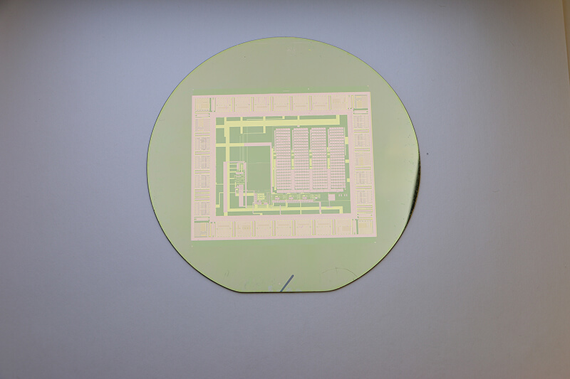 A thin-film electronic circuit can peel easily from its silicon wafer with water, making the wafer reusable for building a nearly infinite number of circuits. (Purdue University image/Chi Hwan Lee)
Download image
A thin-film electronic circuit can peel easily from its silicon wafer with water, making the wafer reusable for building a nearly infinite number of circuits. (Purdue University image/Chi Hwan Lee)
Download image
Eventually, these stickers could also facilitate wireless communication. The researchers demonstrate capabilities on various objects in a paper recently published in the Proceedings of the National Academy of Sciences. A YouTube video is available at https://youtu.be/8tNrPVi4OGg.
"We could customize a sensor, stick it onto a drone, and send the drone to dangerous areas to detect gas leaks, for example," said Chi Hwan Lee, Purdue assistant professor of biomedical engineering and mechanical engineering.
Most of today’s electronic circuits are individually built on their own silicon “wafer,” a flat and rigid substrate. The silicon wafer can then withstand the high temperatures and chemical etching that are used to remove the circuits from the wafer.
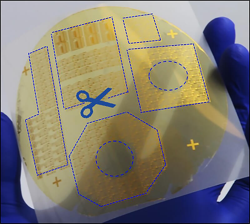 Researchers have designed peelable electronic films that can be cut and pasted onto any object to achieve desired functions. (Purdue University image/Chi Hwan Lee)
Download image
Researchers have designed peelable electronic films that can be cut and pasted onto any object to achieve desired functions. (Purdue University image/Chi Hwan Lee)
Download image
But high temperatures and etching damage the silicon wafer, forcing the manufacturing process to accommodate an entirely new wafer each time.
Lee’s new fabrication technique, called “transfer printing,” cuts down manufacturing costs by using a single wafer to build a nearly infinite number of thin films holding electronic circuits. Instead of high temperatures and chemicals, the film can peel off at room temperature with the energy-saving help of simply water.
“It’s like the red paint on San Francisco’s Golden Gate Bridge – paint peels because the environment is very wet,” Lee said. “So in our case, submerging the wafer and completed circuit in water significantly reduces the mechanical peeling stress and is environmentally friendly.”
A ductile metal layer, such as nickel, inserted between the electronic film and the silicon wafer, makes the peeling possible in water. These thin-film electronics can then be trimmed and pasted onto any surface, granting that object electronic features.
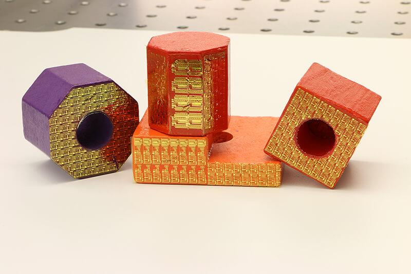 Electronic stickers can turn ordinary toy blocks into high-tech sensors within the ‘Internet of Things.’ (Purdue University image/Chi Hwan Lee)
Download image
Electronic stickers can turn ordinary toy blocks into high-tech sensors within the ‘Internet of Things.’ (Purdue University image/Chi Hwan Lee)
Download image
Putting one of the stickers on a flower pot, for example, made that flower pot capable of sensing temperature changes that could affect the plant’s growth.
Lee’s lab also demonstrated that the components of electronic integrated circuits work just as well before and after they were made into a thin film peeled from a silicon wafer. The researchers used one film to turn on and off an LED light display.
“We’ve optimized this process so that we can delaminate electronic films from wafers in a defect-free manner,” Lee said.
This technology holds a non-provisional U.S. patent. The work was supported by the Purdue Research Foundation, the Air Force Research Laboratory (AFRL-S-114-054-002), the National Science Foundation (NSF-CMMI-1728149) and the University of Virginia.
Writer: Kayla Wiles, 765-494-2432, wiles5@purdue.edu
Source: Chi Hwan Lee, 765-494-6212, lee2270@purdue.edu
Note to Journalists: For a full-text copy of the paper, please contact Kayla Wiles, Purdue News Service, at wiles5@purdue.edu. A YouTube video is available at https://youtu.be/8tNrPVi4OGg, and other multimedia can be found in a Google Drive folder at https://goo.gl/ctaYux. The materials were prepared by Erin Easterling, digital producer for the Purdue College of Engineering, 765-496-3388, easterling@purdue.edu
ABSTRACT
Wafer-recyclable, environment-friendly transfer printing for large-scale thin film nanoelectronics
Dae Seung Wiea1, Yue Zhangb2, Min Ku Kim1, Bongjoong Kim1, Sangwook Park3, Young-Joon Kim1, Pedro P. Irazoqui1, Xiaolin Zheng3, Baoxing Xu2, Chi Hwan Lee1
1Purdue University, West Lafayette, IN, USA
2University of Virginia, Charlottesville, VA, USA
3Stanford University, Stanford, CA, USA
Transfer printing of thin film nanoelectronics from their fabrication wafer commonly requires chemical etching on the sacrifice of wafer, but is also limited by defects with a low yield. Here, we introduce a wafer-recyclable, environment-friendly transfer printing process that enables the wafer-scale separation of high-performance thin film nanoelectronics from their fabrication wafer in a defect-free manner that enables multiple reuses of the wafer. The interfacial delamination is enabled through a controllable cracking phenomenon in a water environment at room temperature. The physically liberated thin film nanoelectronics can be then pasted onto arbitrary places of interest, thereby endowing the particular surface with desirable add-on electronic features. Systematic experimental, theoretical and computational studies reveal the underlying mechanics mechanism and guide manufacturability for the transfer printing process in terms of scalability, controllability, and reproducibility.
