Research
Research » 2D Materials » Band-to-Band Tunneling
While the continued scaling of transistor dimensions has kept pace with Moore’s law, voltages applied to these devices have not scaled in tandem, giving rise to ever-increasing heating challenges in state-of-the-art integrated circuits. This scaling mismatch is due to the thermal limit – the 60mV/decade minimum subthreshold swing (SS) requirement – imposed on transistors that rely on the mechanism of thermal emission (prevalent in modern day CMOS-based electronics) to transition between the ON- and OFF-states. The inability to scale voltages beyond this limit poses a major challenge for future technology nodes. The tunneling field-effect transistor (TFET), which works based on the principle of energy filtering, has been identified as a promising low-power alternative. Two dimensional transition metal dichalcogenides (TMDs) are a promising set of materials for the channel in TFETs owing to their inherent 2D nature which provides excellent electrostatic integrity and the choice of bandgaps and carrier effective masses.
Low-power efforts in the Appenzeller Group have centered on improving ON-state currents and minimizing the subthreshold swing in TFETs through exploration of 2D materials and development of novel fabrication techniques/processes. The following summaries highlight some of the progress made.
Band-to-Band Tunneling in WSe2 Transistor
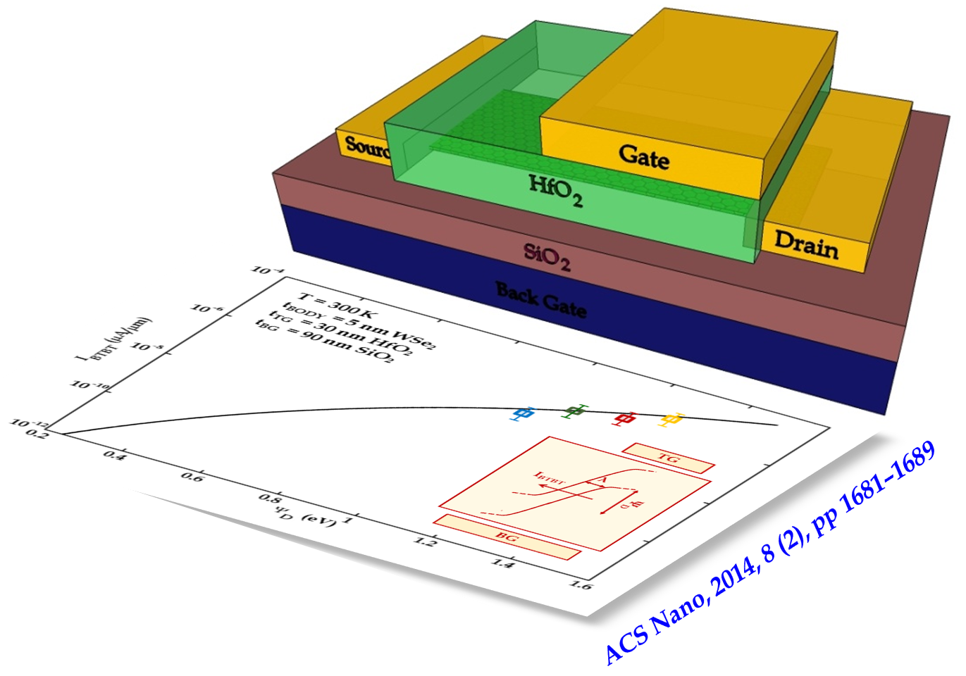
Working on TFETs based on TMDs in the pursuit of realizing a low-power device which can potentially become the building block for future generations of nanoelectronics devices, we have reported for the first time, band-to-band tunneling in double gated WSe2 transistors (see . ACS nano 8, 1681-1689 (2014)). We further improved the ON current levels to as high as 9μA/μm and obtained sub-threshold swing (SS) values as low as 59mV/dec by employing much stronger gates with an equivalent oxide thickness (EOT) in the sub-nanometer regime (results yet to be published).
Authors: Saptarshi Das, Abhijith Prakash, Ramon Salazar
Pictures adapted with permission from ACS nano 8, 1681-1689 (2014). Copyright © 2014 American Chemical Society.
Bandgap Engineering of TMD Materials
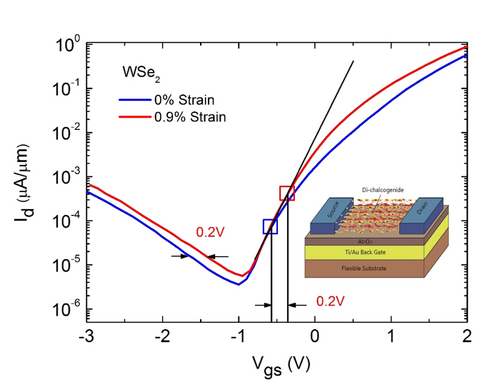
To maximize the efficiency of charge tunneling and achieve highly desirable on-current levels in TMD TFETs, we introduced strain engineering to decrease the band gap of existing TMD materials, such as MoS2 and WSe2. By carefully quantitatively analyzing electrical device characteristics, we were able to demonstrate a 100 meV band gap decrease in multilayer WSe2 under 1.35% uniaxial tensile strain at room-temperature in an FET configuration. Our electrical characterization of strain induced band gap tunability in TMDs presents an important advance toward tuning the band structure of TMDs via strain engineering in particular for TFET applications and also shines some light on how the conduction and valence band edges are impacted by strain in detail. (see ACS Nano 10, 4712-4718 (2016). ).
Authors: Tingting Shen, Ashish Penumatcha
Picture adapted with permission from ACS Nano 10, 4712-4718 (2016). Copyright © 2016 American Chemical Society.
Doping of TMD Materials
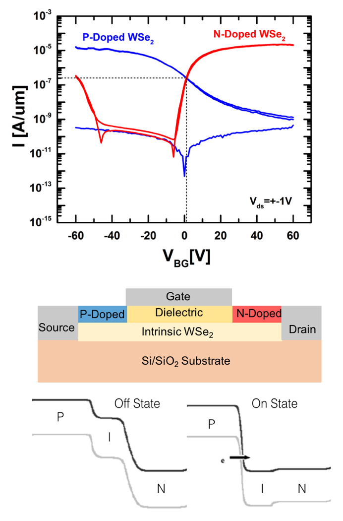
Transition metal dichalcogenides (TMDs) have generated much attention as a potential channel material for ultra-scaled field-effect transistors (FETs). We are investigating modulating the electrical properties of TMDs by methods of chemical doping. In this project, we explored a variety of n- and p-type molecular dopants on WSe2 devices and demonstrate the ability to adjust the channel doping levels. Intrinsic WSe2 shows ambipolar characteristics with the off-state generally around zero volt. We are able to reach sub-uA hole/electron current, under the same back gate condition, after applying n-type and p-type dopants. Currently, we are working on the implementation of chemically doped TMD tunnel FET.
Meanwhile, we are also collaborating with other research groups to explore other doping methods for TMDs (see Nano Letters 16, 5437–5443 (2016))
Authors: Suki Zhang, Abhijith Prakash