Research
Research » 2D Materials
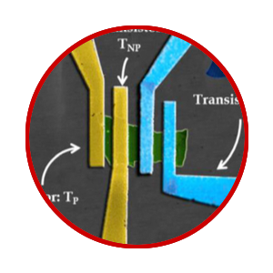
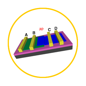
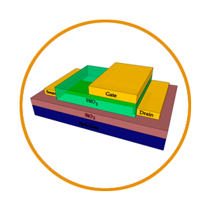
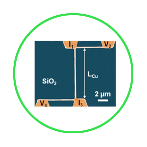
Since the exploration of graphene in 2004, 2D materials have attracted much attention in the scientific community. Recently, 2D semiconductors with a bandgap, such as transition metal dichacolgenides (TMDs) and black phosphorus, are widely explored for various electronic and optoelectronic applications. Due to their atomically thin nature, 2D materials enable device structures and applications beyond conventional 3D materials, such as ultra-scaled atomically-thin channels for FETs and tunneling FETs, vertical stacked heterostructures, etc. Our group studies the properties of 2D materials, including electron transport, contacts, interfaces, etc., and explores their applications in nanoelectronic devices.
To learn more about individual project activities, simply click on the theme buttons below:


