'Inverse opal' structure improves thin-film solar cells
January 13, 2014
 |
|
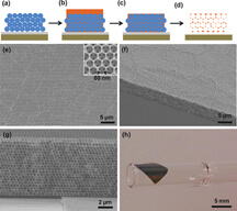
The illustrations at the top (steps A through D) depict the creation of 3-D "photonic crystals" to improve the efficiency of thin-film solar cells, a technology that could bring low-cost solar energy. The "inverse opal" structure is formed by treating the crystals with hydrofluoric acid (d). Scanning electron microscope images show its small-scale crystal structure from three different angles (e and g), and a photograph (h) shows how the same membrane can be wrapped around a glass pipette. (Purdue University image/ Leo Tom Varghese) Download Photo |
WEST LAFAYETTE, Ind. — Researchers have shown how to increase the efficiency of thin-film solar cells, a technology that could bring low-cost solar energy. The approach uses 3-D "photonic crystals" to absorb more sunlight than conventional thin-film cells.
The synthetic crystals possess a structure called an "inverse opal" to make use of and enhance properties found in the gemstones to reflect, diffract and bend incoming sunlight.
"Usually, in thin-film silicon solar cells much of the sunlight comes right back out, but using our approach the light comes in and it is diffracted, causing it to propagate in a parallel path within the film," said Peter Bermel, an assistant professor in Purdue University's School of Electrical and Computer Engineering and Birck Nanotechnology Center.
Compared to solar cells made of silicon wafers, cost is reduced 100 times for the thin films. However, they are less efficient.
"The question is, can we make up that lower efficiency by introducing new approaches to light trapping for thin film solar cells?" Bermel said. "Can we combine low cost and high performance?"
The researchers are the first to demonstrate incorporation of the 3-D photonic crystals to increase light trapping in crystalline silicon solar cells. Experimental findings indicate roughly a 10 percent increase in efficiency over conventional silicon thin films, with further potential for improvement.
The technology is better at absorbing and harvesting near-infrared light.
"A major reason thin-film silicon solar cells have lower efficiency is that they don't absorb near-infrared light very effectively," Bermel said. "Light in the near-infrared range is important because there is a lot of solar energy in that wavelength range and also because silicon can convert near infrared light to energy if it can absorb it, but thin films don't fully absorb it."
Findings were detailed in a research paper appearing in October in the peer-reviewed scientific journal Advanced Optical Materials.
The paper was authored by doctoral student Leo T. Varghese, who has graduated; research professor Yi Xuan; doctoral student Ben Niu; former doctoral student Li Fan, who also has graduated; Bermel; and Minghao Qi, an associate professor of electrical and computer engineering.
The researchers created inverse opals using a process called meniscus-driven self-assembly.
"You could make them to custom order or design, and we decided to make them for solar cells in order to improve absorption of light," Qi said.
Silicon has for many years been the dominant material used in solar cells. However, solar cells made of thick monocrystalline silicon wafers are too expensive to be practical for widespread application. This limitation has driven recent innovation in multicrystalline and thin-film silicon solar cells.
"Our premise is to use only 1 percent as much material as a silicon wafer using these thin films of crystalline silicon," Qi said.
Applications for thin-film solar cells include generating electricity for utilities and the home, as well as smaller-scale applications such as mobile charging of electronic devices.
Natural opals create rainbow patterns caused when different wavelengths of light are diffracted at different angles. Opals are made of solid silica spheres in a matrix of some other material. The new synthetic structures are called inverse opals because they consist of hollow spheres of air surrounded by silicon.
The researchers first build a standard opal structure. The spheres are placed in a solution, which evaporates, leaving the self-assembled structure.
"As it evaporates the spheres get stacked on top of the substrate right at the meniscus, the interface between the liquid and air," Varghese said.
Manufacturers now increase light absorption by etching or depositing random textures on the thin films.
"We think it is best to combine both the textured randomness as well as ordered structure," Bermel said. "The texture helps well with some wavelengths and the ordered structure will help with others."
The research was funded by the U.S. Department of Energy, the Defense Threat Reduction Agency, the Air Force Office of Scientific Research, the National Institutes of Health, and National Science Foundation.
Writer: Emil Venere, 765-494-4709, venere@purdue.edu
Sources: Peter Bermel, 765-496-7879, pbermel@purdue.edu
Minghao Qi, 765-494-3646, mqi@purdue.edu
Leo T. Varghese, vleotom@gmail.com
Note to Journalists: An electronic copy of the research paper is available by contacting Emil Venere, 765-494-4709, venere@purdue.edu
ABSTRACT
Enhanced Photon Management of Thin-Film Silicon Solar Cells Using Inverse Opal Photonic Crystals with 3D Photonic Bandgaps
Leo T. Varghese , Yi Xuan , Ben Niu, Li Fan , Peter Bermel ,* and Minghao Qi *
While silicon (Si) is the most widely used material for solar energy harvesting, it suffers from having an indirect bandgap, which dictates that a relatively thick Si material is required to absorb a significant portion of the solar spectrum. With cost a major concern for the photovoltaic industry, thinner films with enhancements in material efficiency are critical to drive down production costs. This is possible by increasing the path length of light in Si through the use of efficient light-trapping schemes. Traditional optical path length enhancement is based on geometric optics through the use of texturing, which treats all wavelengths equally. An alternative approach based on wave optics is promising because it targets certain wavelengths in the near-IR, where it is most needed for Si. There has been extensive work in integrating plasmonics, gratings, and 1-D distributed Bragg reflectors to improve light trapping. The use of 3-D photonic crystals (PhCs) as back reflectors has been proposed for thin-film crystalline Si solar cells for their superior performance with just a few layers. Previous demonstrations using 3-D PhCs as back reflectors were only performed on dye-sensitized solar cells, or as intermediate reflectors on tandem solar cells. Direct integration of 3-D PhCs on crystalline Si solar cells as back reflectors has never been demonstrated due to the difficulties in incorporating PhCs with Si solar cells or the lack of high-quality PhCs targeting near-IR wavelengths. In this work, we consider a novel experimental approach to improving the performance of thin-film (1.5 micrometer) crystalline silicon-based solar cells that combines the broadband response of textured light trapping with the optimally tailored design of photonic crystal-based light trapping structures.
