'Nano machine shop' shapes nanowires, ultrathin films
August 29, 2012
 |
|
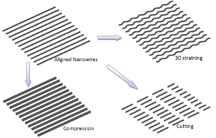
This illustration depicts a new nano machine shop's
ability to shape tiny wires, an advance that represents a possible future
manufacturing method for applications ranging from high-speed electronics to
solar cells. (Purdue University image/Gary Cheng) |
WEST LAFAYETTE, Ind. – A new "nano machine shop" that shapes nanowires and ultrathin films could represent a future manufacturing method for tiny structures with potentially revolutionary properties.
The structures might be tuned for applications ranging from high-speed electronics to solar cells and also may have greater strength and unusual traits such as ultrahigh magnetism and "plasmonic resonance," which could lead to improved optics, computers and electronics.
The researchers used their technique to stamp nano- and microgears; form tiny circular shapes out of a material called graphene, an ultrathin sheet of carbon that holds promise for advanced technologies; and change the shape of silver nanowires, said Gary Cheng, an associate professor of industrial engineering at Purdue University.
"We do this shaping at room temperature and atmospheric pressure, like a nano-machine shop," said Cheng, who is working with doctoral students Ji Li, Yiliang Liao, Ting-Fung Chung and Sergey Suslov and physics professor Yong P. Chen.
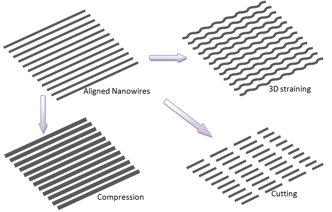
Graphene and nanowires – filaments 1,000 times thinner than a human hair – have numerous potential applications. However, technologies are needed to tailor them for specific uses. The new method, called laser shock-induced shaping, makes it possible to tune nanowires by altering electrical and optoelectrical properties that are critical for electronic components.
The researchers also have shown how laser shock-induced shaping can be used to change the properties of graphene, a step toward harnessing the material for electronic applications.
Findings were detailed in research papers published in the journal Nano Letters, and the work also was highlighted earlier this month in the News and Views section of the journal Nature Photonics. (The article is available at http://www.nature.com/nphoton/journal/v6/n8/full/nphoton.2012.186.html)
The technique works by using a multilayered sandwich structure that has a tiny mold at the bottom. Nanowires were situated directly above the mold, and other materials were layered between the nanowires and a glass cover sheet. Exposing this layered "forming unit" to an ultra-fast pulsing laser causes one of the layers to burn up, generating a downward pressure that forces the nanowires into the mold and changes their shape.
"The process could be scaled up for an industrial roll-to-roll manufacturing process by changing laser beam size and scanning speed," Cheng said. "The laser shock-induced shaping approach is fast and low-cost."
Part of the research, funded by the National Science Foundation, was carried out in a specialized clean room at the Birck Nanotechnology Center in Purdue's Discovery Park.
Writer: Emil Venere, 765-494-4709, venere@purdue.edu
Source: Gary J. Cheng, 765-494-5436, gjcheng@purdue.edu
Note to Journalists: Copies of the research papers are available by contacting Emil Venere, 765-494-4709, venere@purdue.edu
ABSTRACT
Nanoscale Strainability of Graphene by Laser Shock Induced 3D Shaping
Ji Li 1,2, Ting-Fung Chung 3, Yong P. Chen 1,3,4, Gary J. Cheng *1,2
1 Birck Nanotechnology Center, Purdue University
2 School of Industrial Engineering
3 School of Electrical and Computer Engineering
4 Department of Physics
Graphene has many promising physical properties. It has been discovered that local strain in a graphene sheet can alter its conducting properties and transport gaps. It is of great importance to develop scalable strain engineering techniques to control the local strains in graphene and understand the limit of the strains. Here, we present a scalable manufacturing process to generate 3-D nanostructures and thus induce local strains in the graphene sheet. This process utilizes laser induced shock pressure to generate 3-D tunable straining the graphene sheet. The size dependent straining limit of the graphene and the critical breaking pressure are both studied. It is found that the graphene film can be formed to a circular mold (~50nm in diameter) with an aspect ratio of 0.25 and strain of 12%, and the critical breaking pressure is 1.77GPa. These values were found to be decreasing with the increase of mold size. The local straining and breaking of graphene film are verified by Raman spectra. Large scale processing of the graphene sheet into nano-scale patterns is presented. The process could be scaled up to roll-to-roll process by changing laser beam size and scanning speed. The presented laser shock straining approach is a fast, tunable and low-cost technique to realize strain engineering of graphene for its applications in nano-electrical devices.
ABSTRACT
Laser Shock-Based Platform for Controllable Forming of Nanowires
Ji Li, Yiliang Liao, Sergey Suslov, and Gary J. Cheng*
Birck Nanotechnology Center and School of Industrial Engineering, Purdue University
One-dimensional nanomaterials have attracted a great deal of research interest in the past few decades due to their unique mechanical, electrical and optical properties. Changing the shape of nanowires (NWs) is both challenging and crucial to change the property and open wide functions of NWs, such as strain engineering, electronic transport, mechanical properties, band structure and quantum properties, etc. Here we report a scalable strategy to conduct cutting, bending and periodic straining of NWs by making use of laser shock pressure. Three-dimensional shaping of silver NWs is demonstrated, during which the Ag NWs exhibit very good ductility (strain-to-failure reaches 110%). Meanwhile, the high electrical conductivity of Ag NWs could retain well under controlled laser shock pressure. The microstructure observation indicates that the main deformation mechanism in Ag NWs under dynamic loading is formation of twinning and stacking fault, while dislocation motion and pile-up is less obvious. This method could be applied to semiconductor NWs as well.
