PhD student’s materials engineering research offers glimpse into challenges of electronic device miniaturization

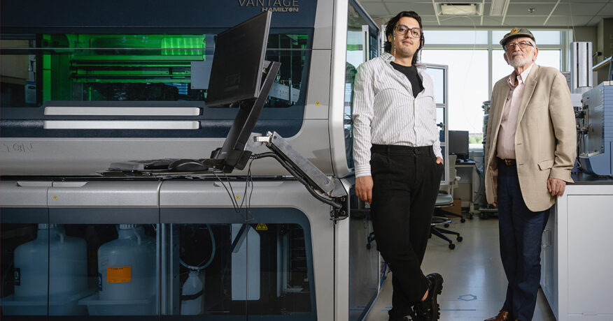
Purdue doctoral student Amey Luktuke is researching the solidification behavior of new, lower temperature interconnects in electronic packaging. With its proximity to Purdue’s West Lafayette campus, he used advanced X-ray imaging techniques available at the synchrotron at the Advanced Photon Source of the Argonne National Laboratory. (Purdue University photo provided)
Amey Luktuke, a graduate research assistant in materials engineering at Purdue, recently defended his PhD thesis addressing the effects of miniaturization of electronic devices. In simple terms, in smartphones, computers and other electronic devices, there are multiple components including microchips, transistors and more.
Electronic packaging encompasses the process of enclosing, safeguarding or establishing the physical framework for electronic components or finalized electronic devices. The electronic package serves as a framework that binds these components together, resulting in the creation of a high-performance device.
For decades, the size of an electronic device was determined by the size of a transistor. As the size of a transistor decreased, the device itself also became smaller. Reducing the transistor size further, however, poses significant physical limitations. Therefore, a lot of attention has been given to packaging strategies. Using such strategies, the trend of miniaturization could be continued.
Luktuke says that with the increasingly higher density of interconnects in an electronic package, very dissimilar materials will be sitting next to each other (a lower melting point polymer next to a much higher melting point metal, for example).
He is working to understand the solidification behavior of new, lower temperature interconnects in electronic packaging using advanced X-ray imaging techniques available at the synchrotron at the Advanced Photon Source of the Argonne National Laboratory.

Purdue has a long relationship with Argonne, the nation’s first national laboratory where students, faculty and industry experts can conduct leading-edge basic and applied scientific research in virtually every scientific discipline.
Many Purdue alumni, including 2023 Distinguished Engineering Alumna Valerie Taylor, who is director of the Mathematics and Computer Science Division at Argonne, work at the laboratory, which is located just two hours north of the West Lafayette campus and southwest of Chicago.
Luktuke began his doctoral studies in 2018 at Arizona State University in professor Nikhilesh Chawla’s research group. When Chawla, the Ransburg Professor in Materials Engineering, joined the Purdue faculty in 2020, he presented an opportunity for Luktuke to continue his doctoral studies at Purdue.
“To be honest, it was an easy decision for me to come to Purdue,” Luktuke says. “I was well aware of Purdue University’s remarkable research environment, outstanding facilities and the extensive engineering legacy it holds. Moreover, I was able to continue the same research that I started at ASU.”
Research tests metallic alloys in the solder connections
Luktuke’s research has focused on solder alloys that can be used for advanced electronic packaging.
Heterogeneous integration packaging (HIP) has emerged as a promising strategy because it not only reduces the size of electronic devices but also enhances their overall performance. HIP involves integrating separately manufactured components into a higher-level assembly. Solder joints are used to provide electrical connections between various components. This is done by melting the alloy between those components and solidifying them to form a connection.
In the advanced packages, solder alloys are positioned in close proximity to lower melting temperature materials like polymers. Commonly used tin-silver-copper (Sn-Ag-Cu) solder alloys, which require high-processing temperatures (>240˚C), can cause significant thermal warpage due to the differences in thermal expansion coefficients of these materials.
To tackle this issue, employing low melting point solder alloys such as tin-indium (Sn-In) and tin-bismuth (Sn-Bi) is an effective solution because it allows for a reduction in reflow temperature.
“Reducing the overall size of a device also affects the solder properties and ultimately the reliability of the device,” Luktuke says. “For example, the smaller size of solder joints means that they will carry higher current densities. This can lead to high heat buildup in the package due to Joule heating. Moreover, the solders are also prone to electromigration damage.”
To form an electrical connection between the components, the solder alloys are melted and solidified. Luktuke’s research focuses on understanding how this solidification process influences the formation of microstructures in these solder alloys. These microstructures affect the mechanical, electrical and thermal properties of the joints. Therefore, it is critical to understand the mechanisms behind their formations.
He says most of the previous studies have been limited to analyzing the 2D images of the solidified structures using traditional electron microscopy methods.
“This limits our knowledge of the shapes, sizes and distribution of microstructural features such as phases that form during solidification. The use of advanced X-ray imaging techniques, such as synchrotron X-ray tomography, at Argonne National Laboratory offers a distinctive approach to nondestructively assess the 3D microstructure,” Luktuke says.
“Moreover, it enables rapid capture of changes occurring during solidification, thereby enhancing our analysis to a four-dimensional perspective (3D microstructure over solidification time),” he adds. “However, such 4D experiments on high-density solder alloys such as tin-bismuth are extremely difficult due to various experimental challenges. During my PhD, we successfully conducted the 4D investigation of solidification process at ANL.”
Luktuke says that for the first time, he observed a unique pyramidal morphology of Bi forming in the solder alloy. This experimental methodology developed in this work has the potential to be extended to investigate a wide range of alloy solidification mechanisms, enabling a deeper understanding of these materials.
“The nondestructive X-ray tomography characterization allowed us to visualize, for the first time, the precise pyramidal morphology of Bi particles. With our 4D-solidification study, we were able to identify the fundamental mechanisms behind the formation of such pyramidal Bi particles,” Luktuke says.
“On the other hand, the experimental methodology we developed in conjunction with collaborators at 7-BM beamline at Argonne National Laboratory could be used to understand various alloy solidification mechanisms which hold important engineering applications.”
Writer: Della Pacheco, dpachec@purdue.edu
Research News

At the nation’s only all-digital nuclear reactor, engineers conduct the first experiments of their kind in the U.S.
July 10, 2026

Purdue engineers test, validate novel method to improve pharmaceutical R&D
June 22, 2026
Purdue researchers work to accelerate cancer drug discovery with next-gen tech platform
June 17, 2026

Purdue Institute for Cancer Research secures $9.4M in renewal of its National Cancer Institute Cancer Center Support Grant
June 11, 2026