Silicon alternatives key to future computers, consumer electronics
June 4, 2014
 |
|
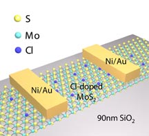
This graphic depicts the structure of an extremely thin semiconductor called molybdenum disulfide, which is particularly promising for future flexible and transparent electronic devices for displays, touch pads and other applications. The structure of molybdenum disulfide is a single-atomic layer of molybdenum sandwiched between single-atomic layers of sulfide and "doped" with a chemical compound called 1,2 dichloroethane (DCE). (Purdue University photo/Lingming Yang) |
WEST LAFAYETTE, Ind. – Researchers are reporting key milestones in developing new semiconductors to potentially replace silicon in future computer chips and for applications in flexible electronics.
Findings are detailed in three technical papers, including one focusing on a collaboration of researchers from Purdue University, Intel Corp. and SEMATECH, a consortium dedicated to advancing chip manufacturing. The team has demonstrated the potential promise of an extremely thin - or "two-dimensional" - semiconductor called molybdenum disulfide.
Although molybdenum disulfide has been studied by research groups around the world, a key obstacle to its practical use has been a large electrical resistance between metal contacts and single-atomic layers of the material. This "contact resistance" limits the flow of current between the contacts and the molybdenum disulfide, hindering performance.
"This is a fundamental bottleneck," said Peide "Peter" Ye, a Purdue professor of electrical and computer engineering.
Now, researchers have shown how to overcome this obstacle by "doping" the material with the chemical compound 1,2 dichloroethane (DCE), meaning single layers of molybdenum disulfide are impregnated with the DCE. This doping results in a 10-fold reduction of contact resistance and a 100-fold reduction of contact resistivity, another measure of resistance.
The findings are fundamental to learning how to develop alternatives to silicon that will likely be needed after 2020, when, it is thought, silicon transistors will reach their technological limits, stalling further progress.
Findings will be presented during the 2014 Symposia on VLSI Technology and Circuits on June 9-13 in Honolulu. The paper was authored by Purdue doctoral students Lingming Yang, Yuchen Du, Han Liu and Heng Wu; SEMATECH researchers Kausik Majumdar, Py Hung, Robert Tieckelmann and Chris Hobbs; Michael Hatzistergos, a researcher from State University of New York's College of Nanoscale Science and Engineering; Intel's Wilman Tsai; and Ye.
The structure of molybdenum disulfide is a single-atomic layer of molybdenum sandwiched between single-atomic layers of sulfide. The researchers were able to dope these tiny structures with the DCE.
"It is inherently difficult to dope a single atomic layer," Ye said. "It is much more difficult than doping bulk silicon for conventional semiconductor devices. I think an important factor is the collaboration between academia, Intel and SEMATECH, which has made this kind of research possible."
Researchers call the technique molecular layer doping.
In one respect, the molybdenum disulfide is similar to graphene, an extremely thin layer of carbon, which is promising for applications in electronics and computers. Like graphene, the material forms in one-atom-thick layers that can be peeled away. Unlike graphene, however, the material is a semiconductor, potentially making it practical for electronic devices. It is particularly promising for thin, flexible and transparent electronic devices for displays, touch pads and other applications.
The molybdenum disulfide paper is one of three papers to be presented by Ye's research group during the VLSI conference.
One of the other papers details findings showing the first high-performance devices made using a material called gallium-arsenide, promising for the post-silicon era for future computers and consumer electronics. Such semiconductors are called III-V materials because they combine elements from the third and fifth groups of the periodic table.
The findings show gallium-arsenide is compatible with the complementary metal–oxide–semiconductor (CMOS) manufacturing process used to construct integrated circuits.
"Research on gallium-arsenide MOS has been going on for about 50 years, and here we demonstrated for the first time that it is doable at the CMOS-circuit level," Ye said.
In the third paper, researchers show how to use a semiconductor called germanium to produce two types of transistors needed for electronic devices. The material had previously been limited to "P-type" transistors. The new findings show how to use the material also to make "N-type" transistors "with significantly improved contacts," Ye said. Because both types of transistors are needed for CMOS circuits, the findings point to possible applications for germanium in computers and electronics.
Portions of the research, based at the Birck Nanotechnology Center in Purdue's Discovery Park, are funded by the National Science Foundation, the Semiconductor Research Corp. and SEMATECH.
Writer: Emil Venere, 765-494-4709, venere@purdue.edu
Source: Peide Ye, 765-494-7611, yep@purdue.edu
Note to Journalists: Electronic copies of the research papers are available from Emil Venere, Purdue News Service, at 765-494-4709, venere@purdue.edu
ABSTRACT
High-Performance MoS2 Field-Effect Transistors Enabled by Chloride Doping: Record Low Contact Resistance (0.5 kΩ·µm) and Record High Drain Current (460 µA/µm)
Lingming Yang1, Kausik Majumdar, 2* , Yuchen Du1, Han Liu 1, Heng Wu 1, Michael Hatzistergos3, Py Hung 2 , Robert Tieckelmann 2, Wilman Tsai 4 , Chris Hobbs 2 , and Peide D. Ye1#
1 School of Electrical and Computer Engineering, Purdue University
2 SEMATECH, Albany, NY
3 SUNY CNSE, Albany NY
4 Intel Corporation, Santa Clara, CA
Tel: 1-765-494-7611, Fax: 1-765-496-7443, Email: # yep@purdue.edu , * kausik.majumdar@sematech.org
In this paper, we report a novel chemical doping technique to reduce the contact resistance (Rc) of transition metal dichalcogenides (TMDs) – eliminating two major roadblocks (namely, doping and high Rc) toward demonstration of high-performance TMDs field-effect transistors (FETs). By using 1,2 dichloroethane (DCE) as the doping reagent, we demonstrate an active n-type doping density > 2×10 19 cm -3 in a few-layer MoS2 film. This enabled us to reduce the Rc value to a record low number of 0.5 kΩ·µm, which is ~10 lower than the control sample without doping. The corresponding specific contact resistivity (ρc) is found to decrease by two orders of magnitude. With such low Rc, we demonstrate 100 nm channel length (Lch) MoS2 FET with a drain current (Ids) of 460 µA/µm at Vds = 1.6 V, which is twice the best value reported so far on MoS2 FETs.
ABSTRACT
Ge CMOS: Breakthroughs of nFETs (Imax=714 mA/mm, gmax=590 mS/mm) by recessed channel and S/D
Heng Wu, Mengwei Si, Lin Dong, Jingyun Zhang and Peide D. Ye*
School of Electrical and Computer Engineering, Purdue University
*Tel: 1-765-494-7611, Fax: 1-765-496-6443, Email: yep@purdue.edu
We report a new approach to realize the Ge CMOS technology based on the recessed channel and source/drain (S/D). Both junctionless (JL) nFETs and pFETs are integrated on a common GeOI substrate. The recessed S/D process greatly improves the Ge n-contacts. A record high maximum drain current (Imax) of 714 mA/mm and trans-conductance (gmax) of 590 mS/mm, high Ion/Ioff ratio of 1×10⁵ are archived at channel length (Lch) of 60 nm on the nFETs. Scalability studies on Ge nFETs are conducted in sub-100 nm region down to 25 nm for the first time. Considering the Fermi level (EF) pining near the valence band edge (EV) of Ge, a novel hybrid CMOS structure with the inversion-mode (IM) Ge pFET and the JL accumulation-mode (JAM) Ge nFET is proposed.
ABSTRACT
III-V CMOS Devices and Circuits with High-Quality Atomic-Layer-Epitaxial La2O3/GaAs Interface
L. Dong,1 X.W. Wang,2 J.Y. Zhang,1 X.F. Li,1 X.B. Lou,2 N. Conrad, 1 H. Wu, 1 R.G. Gordon, 2 and P. D. Ye1
1 School of Electrical and Computer Engineering, Purdue University
2 Department of Chemistry and Chemical Biology, Harvard University
Tel: 1-765-494-7611, Fax: 1-765-496-7443, Email: yep@purdue.edu
GaAs, as the most studied III-V semiconductor, has for a long time been considered to replace Si in logic applications [1]. In order to achieve a thermodynamically stable dielectric on GaAs with a high-quality interface, tremendous efforts have been made by different passivation techniques [2-9] since its first publication in 1965 [10]. Recently, we reported high-performance GaAs nMOSFETs with single crystalline La-based oxide dielectrics [11, 12], showing breakthrough in the drive current. In this work, we demonstrate, for the first time, high-performance GaAs-based CMOS devices and circuits (inverters, NAND and NOR logic gates, and five-stage ring oscillators). These devices were enabled by the high-quality interface of single-crystalline La2O3 grown on GaAs(111)A by atomic layer epitaxy (ALE).
