Research: Low-Power Tunnel Devices
While the continued scaling of transistor dimensions has kept pace with Moore’s law, the voltages applied to these devices has not scaled in tandem, giving rise to ever-increasing heating challenges in state-of-the-art integrated circuits. This scaling mismatch is due to the thermal limit – the 60mV/decade minimum subthreshold swing (S) requirement – imposed on transistors that rely on the mechanism of thermal emission (prevalent in modern day CMOS-based electronics) to transition between the ON- and OFF-states. The inability to scale voltages beyond this limit poses a major challenge for future technology nodes. The tunneling field-effect transistor (TFET) has been experimentally identified as a promising low-power alternative. To-date however, the TFET has suffered from major challenges, such as very low ON-state currents that drastically hinder performance and S < 60 mV/decade over only a small range of OFF-state currents that makes it compare unfavorably against the common MOSFET. A comprehensive overview on the operation, progress, and challanges for the TFET can be found here.
Low-power efforts in the Appenzeller Group have centered on improving ON-state currents and minimizing the subthreshold swing in TFETs through exploration of various material systems and development of novel fabrication techniques/processes. The following summaries highlight some of the progress made.
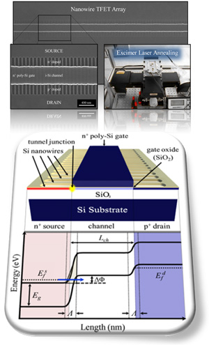
Improved Performance in Silicon Nanowire TFET Arrays Using Excimer Laser Annealing
Applying excimer laser annealing (ELA) in conjunction a low-temperature rapid thermal annealing (LT-RTA) process to activated implanted dopants, the average S of a Si nanowire TFET array are brought to within 9% of the theoretical limit, a 64% reduction over a conventional high-temperature RTA. This improvement is a direct result of preservation of the doping abruptness at the tunnel junction, enabling a smaller tunneling barrier and correspondingly a higher tunneling efficiency. Furthermore, extrapolation of our data through simulation efforts show that future work using this activation process in conjunction with more aggressive yet realistically scaled nanowire TFETs will enable the realization of sub-60 mV/decade operation over three orders of magnitude on a Si platform (see IEEE Trans. Electron Dev., 58, 1822).

Toward Enhanced TFETs Using Ge/Si Core/Shell Nanowires
Back-gated transistors were fabricated from Ge/Si core/shell nanowires with highly doped Si shells. Shells grown at different temperatures showed drastically different morphology and electrical characteristcs. We determined that nanowires with crystalline shell morphologies are suitable for more advanced TFETs, providing an atomically precise doping profile and staggered bandgap alignment – key ingredients for improved tunneling efficiency (see Nano. Lett., 11, 1406).
We have developed a controlled low-temperature wet thermal oxidation process for locally oxidizing portions of these wires that will be used to fabricate the core/shell TFET structure. Results are forthcoming . . .

Broken-Gap Tunnel MOSFET (BG-TMOS)
Low current levels in conventional TFETs have led many researchers to re-examine III-V heterostructures, particularly those with a broken-gap alignment to enable a tunneling probability near unity. In this work, we propose a novel low-power transistor alterative that enables a constant S < 60mV/decade and avoids undesirable features in the output characteristics that are prevalent in the TFET without the 1D restriction. This permits the consideration of 2-D architectures for improved drive current (see IEEE Electron Device Lett., 32, 1367).