Research: Alternative Nanowire Concepts
 Ferroelectric Transistor Random Access Memory (FeTRAM)
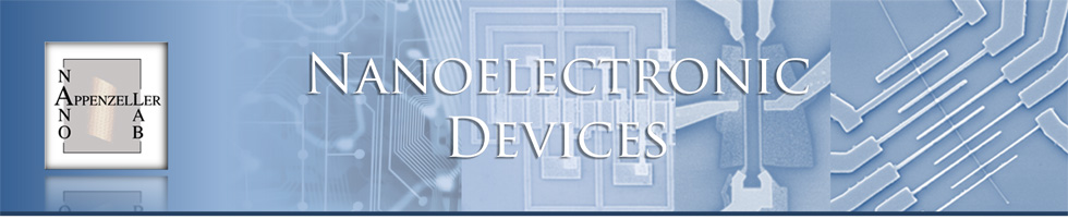
The continued demand for hand-held and personal computing devices has led to the development of a number of durable nonvolitile random access memory (NVRAM) techonologies each with its own advantages and limitations. Ferroelectric materials provide a natural choice for binary-code-based, nonvolatile memory applications, owing to their two inherently stable polarization states, robust lifetime, ultra-fast switching behavior, and potential for low-power operation; however, conventional FeRAM suffers from a destructive readout.
We report the experimental implementation of a novel nonvolatile memory cell, called FeTRAM, that combines silicon nanowires with an organic ferroelectric polymer – PVDF-TrFE – into a new ferroelectric transistor architecture. By replacing the memory capacitor with a memory ferroelectric transistor, the FeTRAM achieves a nondestructive readout (see Nano. Lett., 11, 4003).
 Contact Effects in Silicon Nanowires
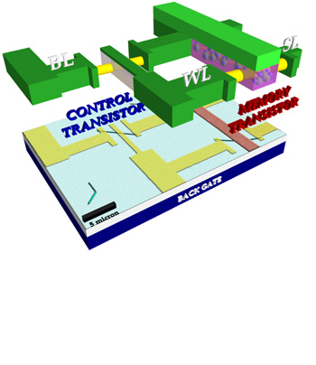
While considerable attention is often given to scaling down channel dimensions of the transistor, comparitively little attention is given to the role that contacts play even though total device scaling includes a reduction in contact size. Further, regardless of the choice of channel material, as transport approaches the ballistic limit the impact of high mobility materials, such as III-V semiconductors, carbon nanotubes, and graphene, no longer play the central role – rather contact resistance becomes the primary performance bottleneck.
To study the influence of contact resistance as contact dimensions are scaled below 100nm lengths, we used e-beam lithography to fabricate sets of scaled contacts along highly doped Si nanowires. Experimental results together with modeling efforts revealed important insights in the scaling behavior (see DRC 2010).
 InSb Nanowire Field-Effect Transistors
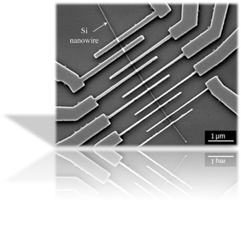
With the smallest band gap and effective mass of the known bulk semiconductors and correspondingly an ultra-high electron mobility at room-temperature, indium antimonide (InSb) holds the potential for low-power, high-speed device applications. At the same time, there is a growing interest in improving the scaling of devices by employing ultra-thin body structures or optimally a nanowire geometry.
Here, we present the first electrical characterization of InSb nanowire field-effect transistors (NWFETs), including a careful analysis of the device characteristics in terms of the bandgap which was deterimined to be in the range of 160-180meV using a simple - yet robust - data analysis technique. The presented device characteristics are a starting point to develop an understanding of InSb NWFETs that can lead to new device architectures such as tunneling field-effect transistors, highly linear amplifiers, and other high-speed, low-power applications (see DRC 2009).