Inkjet-printed liquid metal could bring wearable tech, soft robotics
April 7, 2015
 |
|
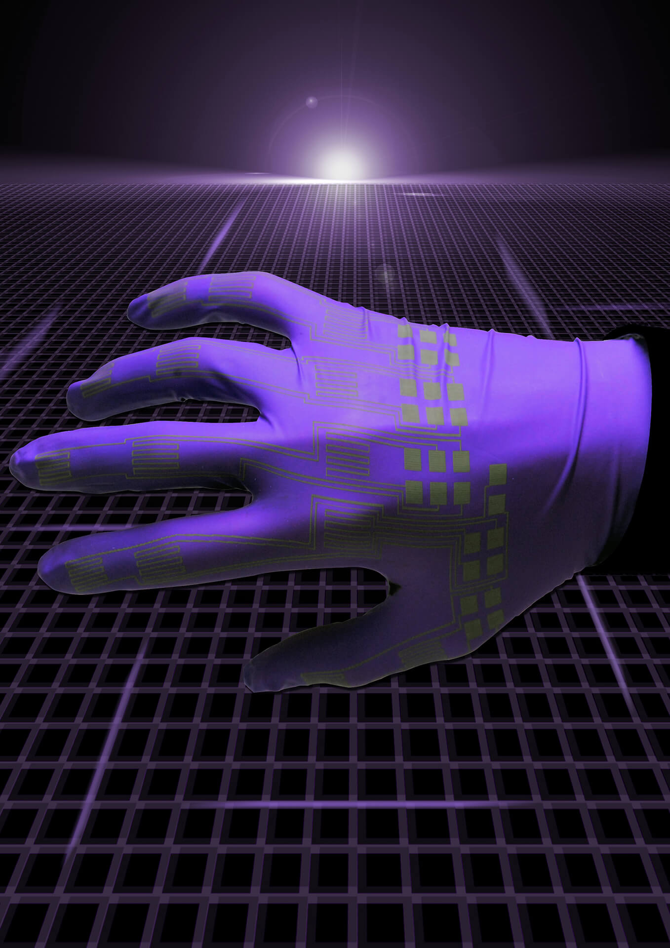
This artistic rendering depicts electronic devices created using a new inkjet-printing technology to produce circuits made of liquid-metal alloys for "soft robots" and flexible electronics. Elastic technologies could make possible a new class of pliable robots and stretchable garments that people might wear to interact with computers or for therapeutic purposes. (Alex Bottiglio/Purdue University |
WEST LAFAYETTE, Ind. — New research shows how inkjet-printing technology can be used to mass-produce electronic circuits made of liquid-metal alloys for "soft robots" and flexible electronics.
Elastic technologies could make possible a new class of pliable robots and stretchable garments that people might wear to interact with computers or for therapeutic purposes. However, new manufacturing techniques must be developed before soft machines become commercially feasible, said Rebecca Kramer, an assistant professor of mechanical engineering at Purdue University.
"We want to create stretchable electronics that might be compatible with soft machines, such as robots that need to squeeze through small spaces, or wearable technologies that aren't restrictive of motion," she said. "Conductors made from liquid metal can stretch and deform without breaking."
A new potential manufacturing approach focuses on harnessing inkjet printing to create devices made of liquid alloys.
"This process now allows us to print flexible and stretchable conductors onto anything, including elastic materials and fabrics," Kramer said.
A research paper about the method will appear on April 18 in the journal Advanced Materials. The paper generally introduces the method, called mechanically sintered gallium-indium nanoparticles, and describes research leading up to the project. It was authored by postdoctoral researcher John William Boley, graduate student Edward L. White and Kramer.
A printable ink is made by dispersing the liquid metal in a non-metallic solvent using ultrasound, which breaks up the bulk liquid metal into nanoparticles. This nanoparticle-filled ink is compatible with inkjet printing.
"Liquid metal in its native form is not inkjet-able," Kramer said. "So what we do is create liquid metal nanoparticles that are small enough to pass through an inkjet nozzle. Sonicating liquid metal in a carrier solvent, such as ethanol, both creates the nanoparticles and disperses them in the solvent. Then we can print the ink onto any substrate. The ethanol evaporates away so we are just left with liquid metal nanoparticles on a surface."
After printing, the nanoparticles must be rejoined by applying light pressure, which renders the material conductive. This step is necessary because the liquid-metal nanoparticles are initially coated with oxidized gallium, which acts as a skin that prevents electrical conductivity.
"But it's a fragile skin, so when you apply pressure it breaks the skin and everything coalesces into one uniform film," Kramer said. "We can do this either by stamping or by dragging something across the surface, such as the sharp edge of a silicon tip."
The approach makes it possible to select which portions to activate depending on particular designs, suggesting that a blank film might be manufactured for a multitude of potential applications.
"We selectively activate what electronics we want to turn on by applying pressure to just those areas," said Kramer, who this year was awarded an Early Career Development award from the National Science Foundation, which supports research to determine how to best develop the liquid-metal ink.
The process could make it possible to rapidly mass-produce large quantities of the film.
Future research will explore how the interaction between the ink and the surface being printed on might be conducive to the production of specific types of devices.
"For example, how do the nanoparticles orient themselves on hydrophobic versus hydrophilic surfaces? How can we formulate the ink and exploit its interaction with a surface to enable self-assembly of the particles?” she said.
The researchers also will study and model how individual particles rupture when pressure is applied, providing information that could allow the manufacture of ultrathin traces and new types of sensors.
Writer: Emil Venere, 765-494-4709, venere@purdue.edu
Source: Rebecca Kramer, 765-494-2219, rebeccakramer@purdue.edu
Note to Journalists: Journalists may obtain a copy of the research paper by contacting Emil Venere, 765-494-4709, venere@purdue.edu.
ABSTRACT
Mechanically Sintered Gallium–Indium Nanoparticles
John William Boley, Edward L. White, and Rebecca K. Kramer*
School of Mechanical Engineering, Purdue University
E-mail: rebeccakramer@purdue.edu
Metallic nanoparticles (MNPs) have been used since ancient times. [1] Recent advancements in science and engineering have demonstrated the utilization of MNPs for applications in a broad array of fields, including optics, [2] medicine, [3] memory, [4–6] and semiconductors. [7] Many current applications require a sintering step in order to coalesce the deposited MNPs to enable functionality; whether it is thermal, [8,9] photonic, [10–12] plasmatic, [13] or chemical in nature. [14–16] Although ambient and local temperatures of current sintering methods are significantly lower than the melting point of the bulk materials, difficulties can still arise when integrating MNPs into functional devices with other materials such as chemically or thermally sensitive polymers. Here, we introduce a new class of MNPs that are "mechanically sintered" at and below room temperature. Using eutectic gallium-indium (EGaIn) MNPs coated with Ga2O3 or thiol, we demonstrate particle coalescence via the application of low pressures, which ruptures the particle coatings and releases the low-viscosity liquid-metal. This phenomenon is observed morphologically through scanning electron imaging and electrically through two-probe measurements during compression. Fusing the results of this study with the unique properties of EGaIn and the semiconductive nature of Ga2O3 [17] will facilitate new applications across a broad array of fields such as soft robotics, conformable electronics, wireless communications, micro/nanofluidics, wearable/implantable devices, and energy storage and transport systems. We also demonstrate that EGaIn MNPs are compatible with scalable additive manufacturing technologies such as inkjet printing and can be used to fabricate flexible/stretchable integrated devices across multiple length scales.
