'Metasurfaces' to usher in new optical technologies
March 14, 2013
 |
|
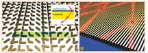
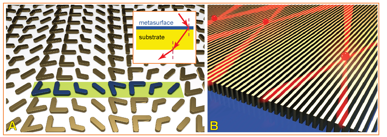
This
schematic view of a nanoantenna array (A), at left, is an example of new
plasmonic metasurfaces that are promising for various advances, including a
possible "hyperlens" that could make optical microscopes 10 times
more powerful. At right (B) is a "hyperbolic metasurface," a tiny
metallic grating for enhancing "quantum emitters," which could make
possible future quantum information systems far more powerful than today's
computers. (Birck Nanotechnology Center, Purdue University)
|
WEST LAFAYETTE, Ind. – New optical technologies using "metasurfaces" capable of the ultra-efficient control of light are nearing commercialization, with potential applications including advanced solar cells, computers, telecommunications, sensors and microscopes.
The metasurfaces could make possible "planar photonics" devices and optical switches small enough to be integrated into computer chips for information processing and telecommunications, said Alexander Kildishev, associate research professor of electrical and computer engineering at Purdue University.
"I think we know enough at this point that we can realistically start to develop prototypes of devices for some applications," he said.
The promise of metasurfaces is described in an article appearing Friday (March 15) in the journal Science. The article was co-authored by Kildishev; Alexandra Boltasseva, an assistant professor of electrical and computer engineering; and Vladimir M. Shalaev, scientific director of nanophotonics at Purdue's Birck Nanotechnology Center and a distinguished professor of electrical and computer engineering.
The metasurfaces are extremely thin films of "metamaterials," assemblies that contain features, patterns or elements such as tiny antennas or alternating layers of oxides that enable an unprecedented control of light. Under development for about 15 years, the metamaterials owe their unusual potential to precision design on the scale of nanometers.
Optical nanophotonic circuits might harness clouds of electrons called "surface plasmons" to manipulate and control the routing of light in devices too tiny for conventional lasers.
The metasurfaces are typically created using electron-beam lithography or focused ion beam milling and may also be made of materials that are compatible with existing semiconductor manufacturing and industrial processes.
"That is one of the attractive features of metasurfaces," Kildishev said. "If we use certain types of plasmonic material, they can be integrated into existing semiconductor processes, which makes them practical for commercialization."
Plasmonic metamaterials are promising for various advances, including a possible "hyperlens" that could make optical microscopes 10 times more powerful; advanced chemical sensors; new types of light-harvesting systems for more efficient solar cells; computers and consumer electronics that use light instead of electronic signals to process information; and a cloak of invisibility.
The metasurfaces can be combined with thin sheets of carbon called graphene.
"If you apply voltage the optical properties of graphene change, and if you couple a graphene layer with a metasurface, these properties then change dramatically," Kildishev said.
Metasurfaces could make it possible to use single photons – the tiny particles that make up light – for switching and routing in future computers. While using photons would dramatically speed up computers and telecommunications, conventional photonic devices cannot be miniaturized because the wavelength of light is too large to fit in tiny components needed for integrated circuits.
Nanostructured metamaterials, however, could make it possible to reduce the size of photons and the wavelength of light, allowing the creation of new types of nanophotonic devices, Shalaev said.
Some of the new materials may have applications involving near-infrared light, the range of the spectrum critical for telecommunications and fiberoptics. Other materials also might work for light in the spectrum's visible range.
Unlike natural materials, metamaterials may possess an index of refraction less than one or less than zero. Refraction occurs as electromagnetic waves, including light, bend when passing from one material into another. It causes the bent-stick-in-water effect, which occurs when a stick placed in a glass of water appears crooked when viewed from the outside. Being able to create materials with an index of refraction that's negative or between one and zero promises a range of potential breakthroughs in a new field called transformation optics.
Development of new technologies using metamaterials has been hindered by two major limitations: too much light is "lost," or absorbed by metals such as silver and gold contained in the metamaterials, and the materials need to be more precisely tuned so that they possess the proper index of refraction. Ultrathin metasurfaces made of novel low-loss plasmonic material components is a promising way to address this challenge.
Researchers are working to replace silver and gold in materials that are created either by making semiconductors more metallic by adding metal impurities to them; or adding non-metallic elements to metals, in effect making them less metallic. Examples of these materials include transparent conducting oxides and titanium nitride, Boltasseva said.
Writer: Emil Venere, 765-494-4709, venere@purdue.edu
Sources: Alexander Kildishev, 765-496-3196, kildishev@purdue.edu
Vladimir Shalaev, 765-494-9855, shalaev@ecn.purdue.edu
Alexandra Boltasseva, 765-494-0301, aeb@purdue.edu
Note to Journalists: A copy of the article is available by contacting the Science Press Package team at 202-326-6440, scipak@aaas.org
ABSTRACT
Planar Photonics with Metasurfaces
Alexander V. Kildishev, Alexandra Boltasseva, Vladimir M. Shalaev*
Metamaterials, or engineered materials with rationally designed, subwavelength-scale building blocks, allow us to control the behavior of physical fields in optical, microwave, radio, acoustic, heat transfer and other applications with flexibility and performance that are unattainable with naturally available materials. In turn, metasurfaces - planar, ultrathin metamaterials - extend these capabilities even further. Optical metasurfaces offer the fascinating possibility of controlling light with surface-confined, flat components. In the planar photonics concept, it is the reduced dimensionality of the optical metasurfaces that enables new physics and, therefore, leads to functionalities and applications that are distinctly different from those achievable with bulk, multilayer metamaterials. Here, we review the progress in developing optical metasurfaces that has occurred over the past few years with an eye toward the promising future directions in the field.
