New '4-D' transistor is preview of future computers
December 4, 2012
 |
|
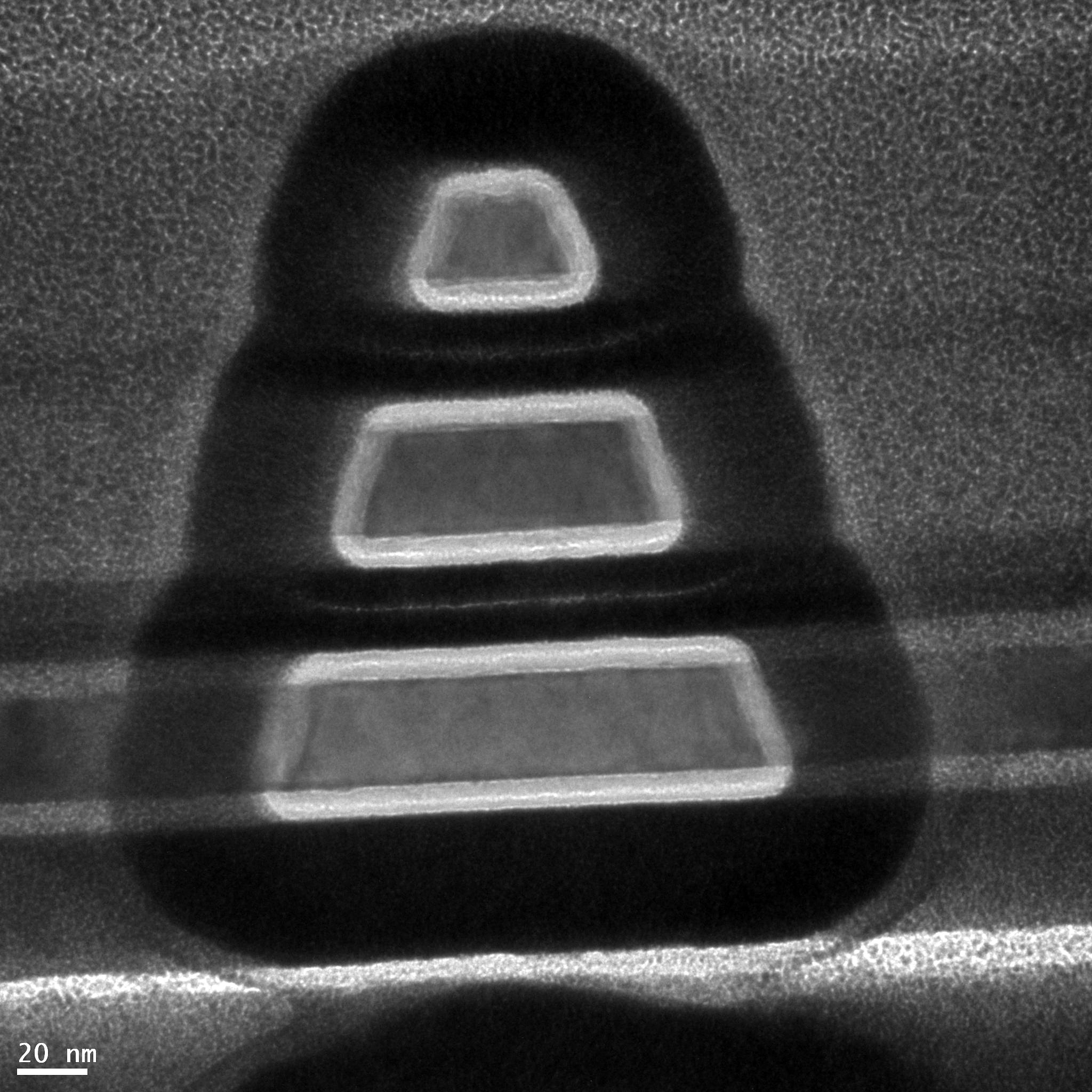
This
image taken with a transmission electron microscope shows the cross section of
a new type of transistor shaped like a Christmas tree that was created by
researchers at Purdue and Harvard universities. The transistor is made from
tiny nanowires of a material called indium-gallium-arsenide, which could
replace silicon within a decade. (Purdue University image) |
WEST LAFAYETTE, Ind. – A new type of transistor shaped like a Christmas tree has arrived just in time for the holidays, but the prototype won't be nestled under the tree along with the other gifts.
"It's a preview of things to come in the semiconductor industry," said Peide "Peter" Ye, a professor of electrical and computer engineering at Purdue University.
Researchers from Purdue and Harvard universities created the transistor, which is made from a material that could replace silicon within a decade. Each transistor contains three tiny nanowires made not of silicon, like conventional transistors, but from a material called indium-gallium-arsenide. The three nanowires are progressively smaller, yielding a tapered cross section resembling a Christmas tree.
The research builds on previous work in which the team created a 3-D structure instead of conventional flat transistors. The approach could enable engineers to build faster, more compact and efficient integrated circuits and lighter laptops that generate less heat than today's.
New findings show how to improve the device performance by linking the transistors vertically in parallel.
"A one-story house can hold so many people, but more floors, more people, and it's the same thing with transistors," Ye said. "Stacking them results in more current and much faster operation for high-speed computing. This adds a whole new dimension, so I call them 4-D."
Findings will be detailed in two papers to be presented during the International Electron Devices Meeting on Dec. 8-12 in San Francisco. One of the papers has been highlighted by conference organizers as among "the most newsworthy topics and papers to be presented."
The work is led by Purdue doctoral student Jiangjiang Gu and Harvard postdoctoral researcher Xinwei Wang.
The newest generation of silicon computer chips, introduced this year, contain transistors having a vertical 3-D structure instead of a conventional flat design. However, because silicon has a limited "electron mobility" - how fast electrons flow - other materials will likely be needed soon to continue advancing transistors with this 3-D approach, Ye said.
Indium-gallium-arsenide is among several promising semiconductors being studied to replace silicon. Such semiconductors are called III-V materials because they combine elements from the third and fifth groups of the periodic table.
The authors of the research papers are Gu; Wang; Purdue doctoral student H. Wu; Purdue postdoctoral research associate J. Shao; Purdue doctoral student A. T. Neal; Michael J. Manfra, Purdue's William F. and Patty J. Miller Associate Professor of Physics; Roy Gordon, Harvard's Thomas D. Cabot Professor of Chemistry; and Ye.
Transistors contain critical components called gates, which enable the devices to switch on and off and to direct the flow of electrical current. Smaller gates make faster operation possible. In today's 3-D silicon transistors, the length of these gates is about 22 nanometers, or billionths of a meter.
The 3-D design is critical because gate lengths of 22 nanometers and smaller do not work well in a flat transistor architecture. Engineers are working to develop transistors that use even smaller gate lengths; 14 nanometers are expected by 2015, and 10 nanometers by 2018.
However, size reductions beyond 10 nanometers and additional performance improvements are likely not possible using silicon, meaning new materials will be needed to continue progress, Ye said.
Creating smaller transistors also will require finding a new type of insulating, or "dielectric" layer that allows the gate to switch off. As gate lengths shrink smaller than 14 nanometers, the dielectric used in conventional transistors fails to perform properly and is said to "leak" electrical charge when the transistor is turned off.
Nanowires in the new transistors are coated with a different type of composite insulator, a 4-nanometer-thick layer of lanthanum aluminate with an ultrathin, half-nanometer layer of aluminum oxide. The new ultrathin dielectric allowed researchers to create transistors made of indium-gallium- arsenide with 20-nanometer gates, which is a milestone, Ye said.
The work, based at the Birck Nanotechnology Center in Purdue's Discovery Park, is funded by the National Science Foundation and the Semiconductor Research Corp.
Writer: Emil Venere, 765-494-4709, venere@purdue.edu
Source: Peide Ye, 765-494-7611, yep@purdue.edu
ABSTRACT
20–80nm Channel Length InGaAs Gate-all-around Nanowire MOSFETs with EOT=1.2nm and Lowest SS=63mV/dec
J. J. Gu,1) X. W. Wang,2) H. Wu,1) J. Shao,3) A. T. Neal,1) M. J. Manfra,3) R. G. Gordon,2) and P. D. Ye 1)
1) School of Electrical and Computer Engineering, Purdue University
2) Department of Chemistry and Chemical Biology, Harvard University
3) Department of Physics, Purdue University,
Recently, a top-down technology for III-V gate-all-around (GAA) nanowire MOSFETs has been demonstrated [1-2]. However, the device metrics such as gm, VDD, SS, DIBL, and the channel length (Lch) scaling of the III-V GAA devices demonstrated in [1] are still greatly limited by the large EOT of the devices. In this abstract, we experimentally demonstrate InGaAs GAA nanowire MOSFETs with an EOT down to 1.2nm by the successful integration of complex oxide dielectric LaAlO3 (k~16) [3]. The reduction of EOT has allowed the demonstration of the first 20nm Lch InGaAs MOSFETs with gm of 1.65mS/μm at Vds=0.5V and negligible short channel effects (SCE). A systematic scaling metrics study with Lch between 20-80nm and nanowire size-dependent transport study with nanowire width (WNW) between 20-35nm has also been carried out for three different gate stacks, demonstrating near-ideal SS of 63mV/dec and DIBL of 7mV/V. It is shown that the integration of 4nm LaAlO3 with ultra-thin 0.5nm Al2O3 interfacial layer allow reduction of EOT=1.2nm with optimized interface trap density (Dit), offering excellent scalability, near-ballistic transport, and high gm at low supply voltage.
ABSTRACT
III-V Gate-all-around Nanowire MOSFET Process Technology: From 3D to 4D
J. J. Gu,1) X. W. Wang,2) J. Shao,3) A. T. Neal,1) M. J. Manfra,3) R. G. Gordon,2) and P. D. Ye 1)
1) School of Electrical and Computer Engineering, Purdue University
2) Department of Chemistry and Chemical Biology, Harvard University
3) Department of Physics, Purdue University,
Introduction: III-V gate-all-around (GAA) nanowire (NW) MOSFETs, or III-V 3D transistors, have been experimentally demonstrated by a top-down approach, showing excellent scalability down to channel length (Lch) of 50nm [1]. However, the gm, SS, and DIBL are greatly limited by the large EOT of the devices [1]. Furthermore, although lateral (parallel to the wafer surface) integration of NWs has been demonstrated with high drive current per wire, the overall current drivability of the devices is limited by the large pitch of the NWs. To overcome this drive current bottleneck, for the first time, a top-down process technology has been developed to fabricate vertically stacked (normal to the wafer surface) III-V NWFETs, similar to some explored Si NWFETs [2-3]. We call this new type of nanowire devices III-V 4D transistors to distinguish them from III-V 3D transistors [1] which has only one vertical layer and multiple lateral wires. The experimental results, in this abstract, show that the drive current per wire pitch (Wpitch) is greatly increased from 3D to 4D structure. The new device concept is very promising for future high-speed low-power logic and RF applications.
