 Purdue News
Purdue News
|
|
|
September 7, 2001 Facility will make Purdue state, national leader in nanotechnologyWEST LAFAYETTE, Ind. – Purdue University today (Friday, 9/7) announced it will build a $100 million Discovery Park and already has raised $51 million for the first building, the Birck Nanotechnology Center, that will be among the best of its kind in the nation.
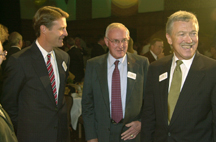
Discovery Park, a new home for interdisciplinary research, also will include a bioscience/engineering center, an e-enterprises center and a center for entrepreneurship. The event, which included a ceremonial groundbreaking, launched Discover Purdue Week, which concludes with the Purdue-Notre Dame football game, Sept. 15. Discover Purdue Week, in turn, kicks off of a yearlong campaign to help Hoosiers "Discover Purdue." Purdue President Martin C. Jischke said the university began the week with Discovery Park because it will play a major role in the state's economy. "This new nanotechnology facility will position Indiana to become a player in the 'Silicon Valley' of the future," Jischke said, noting the state's investment was crucial for the project. "We were able to leverage state funding of $5 million to attract another $46 million in private and federal dollars. "That's the kind of teamwork that gets things done. The Indiana General Assembly's investment has paid off tenfold – a tremendous return on investment. We have many of our elected officials to thank for their foresight, but none more than Pat Bauer, who supported the initiative from start to finish, Bob Meeks who helped in the Senate, Gov. O'Bannon who supplied his leadership and Sen. Bayh, Rep. Kerns and Rep. Buyer who worked for us on Capitol Hill." State Reps. B. Patrick Bauer, D-South Bend, Sheila Klinker, D-Lafayette, and Sue Scholer, R-West Lafayette; and State Sens. Robert Meeks, R-Indianapolis, and Ronnie J. Alting, R-Lafayette; and other members of the State Budget Committee were on hand for the announcement, as were Gov. Frank OąBannon, U.S. Sen. Evan Bayh, D-Ind., Rep. Brian Kerns, R-Ind, and Rep. Steve Buyer, R-Ind. Construction on the three-floor, 71,000-square-foot nanotechnology building is expected to begin in July and be completed in the summer of 2004. The new center will make the university a national leader in nanotechnology, a field that will be critical to science and industry in the 21st century. "Purdue already has dozens of top researchers in nanotechnology," Jischke said. "They are out to prove that, in this case, if you want to think big, first you need to think small." Nanotechnology will have numerous applications in everything from super-small computers, spacecraft and microscopic machines, to tiny life-saving medical devices and a plethora of new materials. In addition to state and other money, the new facility is being funded by $40 million from two couples. Michael and Katherine (Kay) Birck, of Hinsdale, Ill., for whom the facility will be named, have donated $30 million. A Purdue alumnus and a member of the Purdue Board of Trustees, Michael Birck is chairman of Tellabs Inc., which develops and manufactures special telecommunications equipment, in Lisle, Ill. Kay Birck is head of nursing at Women's Healthcare of Hinsdale. Donald and Carol Scifres, Greater Lafayette natives, gave $10 million. Donald Scifres is a Purdue alumnus and Silicon Valley entrepreneur. An electrical engineer, he holds more than 130 patents and is co-chairman of the board and chief strategy officer of JDS Uniphase Corp., an optical communications company in San Jose, Calif. In recognition of their gift, Purdue will name a wing of the new nanotechnology facility after Donald Scifres' father, Ray, who was a member of Purdue's electrical engineering staff for 35 years before retiring in 1975. Additional funding is expected to come from a variety of sources, including the federal government. Federal research spending for nanotechnology is expected to increase sharply in coming years. The facility will help Purdue attract millions of dollars of research money, as well as the best scientists, engineers and students, said James Cooper, a professor in electrical and computer engineering. The facility also will help the state of Indiana attract companies in the high-tech sector by providing one of the nation's most advanced laboratories and a core of researchers to develop prototypes and new processes. "Everybody is really enthusiastic about it," said George Adams, a Purdue adjunct associate professor of electrical and computer engineering who headed the facility's planning committee. "Nanotechnology is still in its infancy and not yet dominated by a particular geographic location, as Silicon Valley dominates the computer industry. "That means nobody has a compelling lead at this point, so this is an area in which you can become a big player fairly easily. We have the potential to make Indiana a high-tech region in the United States for this kind of technology." Several leading universities in the United States have large laboratories for nanotechnology research, but those labs were designed primarily for conventional semiconductor processing. The Purdue lab will be among the first in the nation designed specifically for nanotechnology research, making it better suited for the emerging science, Cooper said. The new facility will provide desperately needed laboratory space, including the most advanced "clean rooms," for Purdue researchers. These clean rooms are equipped with special filtration systems to keep the air nearly free of dust particles. Although the dust particles are microscopic, they are actually larger than some of the features in devices built with nanotechnology. That means clean rooms are critical to nanotechnology research. Researchers must wear gowns, gloves, masks and shoe coverings and take elaborate precautions to cleanse themselves before entering the labs. Nano is a prefix meaning one-billionth. A nanometer is one-billionth of a meter, or only about 10 atoms wide. The letter "I" printed here is about one million nanometers wide. Because scientists and engineers are creating devices so small, dust can pose a problem. "If you are trying to make something that is 20 nanometers wide, and a 300-nanometer piece of dust falls on it, that's like having a big rock fall on your experiment," Adams said. "Essentially, in these clean rooms the ceiling is one giant filter. "The air flow is laminar (straight-line) so that it doesn't form eddies or dead spots where dust can collect, and you do your work right at the outflow of the filter, where the air is as free of dust as possible." The new facility will house 14,000 square feet of such clean rooms, compared with the university's current capacity of only about 3,000 square feet of clean room space. The center also will contain about 19,000 square feet of general laboratory space. Temperature, humidity and vibration also will be carefully controlled in the labs. Rising and falling temperature cause equipment to expand and contract. A rise of only 1 degree Celsius causes microscopes to expand the size equivalent to thousands of atoms, making it impossible to carry out nanometer-scale research. Any vibration also makes it impossible to hold equipment still enough to conduct research on the scales needed for nanotechnology research. Another reason for the tight controls is because of chemical processes that will only work well within a small range of temperature and humidity. One of the building's most innovative features will be the placement of chemical and biological processing labs adjacent to and within facilities typically used to make computer microchips, Cooper said. "I don't believe any other facility in the country has this kind of close interdisciplinary linkage between such disparate fields," he said. Cooper said a diverse team of experts was involved in planning the center. "We brought in faculty and staff from chemical engineering, mechanical engineering, physics, chemistry, biology and materials engineering," he said. "We pulled together the various disciplines – people working in almost any aspect of nanotechnology. "As we brought all these people together, the concept of a highly interdisciplinary facility gradually evolved over the past few years." The nanotechnology facility will be located in Purdue's new Discovery Park, an area bounded by State Street on the north, Nimitz Drive on the south, Airport Road on the west and South Intramural Drive on the east. HDR Inc., a worldwide architectural-engineering firm headquartered in Omaha, Neb., is designing the facility. HDR recently designed the Advanced Measurement Laboratory at the National Institute of Standards and Technology, in Gaithersburg, Md. The $235 million NIST lab, which is currently under construction, will be among the most advanced measurement facilities in the world. Writer: Emil Venere, (765) 494-4709, venere@purdue.edu Sources: Martin C. Jischke (765) 494-9708 George Adams, (765) 494-2698, gba@purdue.edu James Cooper, (765) 494-3514, cooperj@ecn.purdue.edu Related information: Related Web sites: Purdue DevelopmentPHOTO CAPTION: A publication-quality photograph is available at the News Service Web site and at the ftp site. Photo ID: Groundbreak2.jpeg NOTE TO JOURNALISTS: Publication-quality photographs of Martin C. Jischke, Michael and Katherine Birck, Donald Scifres, a schematic of Discovery Park and a Discover Purdue logo are available at https://news.uns.purdue.edu or at ftp://ftp.purdue.edu/pub/uns/. They are called: Jischke.M.jpeg, Bircks.jpeg, Scifres.jpeg, Nano.map.jpeg and Disc.Purdue.jpeg.
|
