 Purdue News
Purdue News
|
|
|
November 2001 Purdue launches Discovery Park, nanotechnology centerWEST LAFAYETTE, Ind. – Purdue University has announced it will build a $100 million Discovery Park and already has raised $51 million for the first building, the Birck Nanotechnology Center, which will be among the best of its kind in the nation.
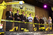
Discovery Park, a new home for interdisciplinary research, also will include a bioscience/engineering center, an e-enterprises center and a center for entrepreneurship. The September event, which included a ceremonial groundbreaking, launched Discover Purdue Week. Discover Purdue Week, in turn, kicks off of a yearlong "Discover Purdue" campaign. Purdue President Martin C. Jischke said the university began the campaign with Discovery Park because it will play a major role in the state's economy. "This new nanotechnology facility will position Indiana to become a player in the 'Silicon Valley' of the future," Jischke said, noting the state's investment was crucial for the project. "We were able to leverage state funding of $5 million to attract another $46 million in private and federal dollars. "That's the kind of teamwork that gets things done. The Indiana General Assembly's investment has paid off tenfold – a tremendous return on investment. We have many of our elected officials to thank for their foresight, but none more than Pat Bauer, who supported the initiative from start to finish, Bob Meeks who helped in the Senate, Gov. O'Bannon who supplied his leadership and Sen. Bayh and Rep. Kerns who worked for us on Capitol Hill. State Reps. B. Patrick Bauer, D-South Bend, Sheila Klinker, D-Lafayette, and Sue Scholer, R-West Lafayette; and State Sens. Robert Meeks, R-Indianapolis, and Ronnie J. Alting, R-Lafayette; and other members of the State Budget Committee were on hand for the announcement, as were Gov. Frank OąBannon, U.S. Sen. Evan Bayh, D-Ind., Rep. Brian Kerns, R-Ind, and Rep. Steve Buyer, R-Ind. Construction on the three-floor, 71,000-square-foot nanotechnology building is expected to begin in July and be completed in the summer of 2004. The new center will make the university a national leader in nanotechnology, a field that will be critical to science and industry in the 21st century. "Purdue already has dozens of top researchers in nanotechnology," Jischke said. "They are out to prove that, in this case, if you want to think big, first you need to think small." Nanotechnology will have numerous applications in everything from super-small computers, spacecraft and microscopic machines, to tiny life-saving medical devices and a plethora of new materials. In addition to the state money, the new facility is being funded by $43 million from two couples. Michael and Katherine (Kay) Birck, of Hinsdale, Ill., for whom the facility is named, have donated $30 million. Michael Birck is chairman of Tellabs Inc., which develops and manufactures special telecommunications equipment and is based in Lisle, Ill. A Purdue alumnus and a member of the Purdue Board of Trustees, Michael Birck is a native of Clinton, Ind. Kay Birck, a native of Terre Haute, Ind., is head of nursing at Women's Healthcare of Hinsdale. Purdue alumni Donald and Carol Scifres, gave $10 million. Donald Scifres, is a Silicon Valley entrepreneur. An electrical engineer, he holds more than 130 patents and is co-chairman of the board and chief strategy officer of JDS Uniphase Corp., an optical communications company in San Jose, Calif. In recognition of their gift, Purdue will name a wing of the new nanotechnology facility after Donald Scifres' father, Ray, who was a member of Purdue's electrical engineering staff for 35 years before retiring in 1975. Donald and Carol Scifres are both Greater Lafayette area natives. Additional funding is expected to come from a variety of sources, including the federal government. Federal research spending for nanotechnology is expected to increase sharply in coming years. The facility will help Purdue attract millions of dollars of research money, as well as the best scientists, engineers and students, said James Cooper, a professor in electrical and computer engineering. The facility also will help the state of Indiana attract companies in the high-tech sector by making the nation's best laboratories and experts available for developing prototypes and new processes. Nanotechnology is an emerging science in which new materials and tiny structures are built atom-by-atom, or molecule-by-molecule, instead of the more conventional approach of sculpting parts from pre-existing materials. Nano is a prefix meaning one-billionth, so a nanometer is one-billionth of a meter. A human red blood cell is about 7,500 nanometers across, and one nanometer is roughly 10 atoms wide. The letter "I" printed here is about one million nanometers wide. Just as antibiotics, the silicon transistor and plastics affected nearly every aspect of society in the 20th century, nanotechnology is expected to have profound influences in the 21st century. The possibilities include: • The creation of entirely new materials with superior strength, electrical conductivity, resistance to heat and other properties. • Microscopic machines for a variety of uses, including probes that could be injected into the body for medical diagnostics and repair. • A new class of ultra-small, super-powerful computers and other electronic devices, including spacecraft. • A technology in which biology and electronics are merged, creating "gene chips" that instantly detect food-borne contamination, dangerous substances in the blood or chemical warfare agents in the air. • Artificial organs. • The development of "molecular electronics" and devices that "self assemble," similar to the growth of complex organic structures in living organisms. Theoretically, once set in motion, such self-assembling devices would build themselves, making electronics processing far less expensive than conventional semiconductor processing. George Adams, a Purdue engineer who headed the facility's planning committee for the nanotechnology center, said Purdue and the state are poised to become a national leader in nanotechnology. "Nanotechnology is an area that is still in its infancy and not yet dominated by a particular geographic location, as Silicon Valley dominates the computer industry. "That means nobody has a compelling lead at this point, so this is an area in which you can become a big player fairly easily. We have the potential to make Indiana a high-tech region in the United States for this kind of technology." Several leading universities in the United States have large laboratories for nanotechnology research, but those labs were designed primarily for conventional semiconductor processing. The Purdue lab will be designed specifically for nanotechnology research, making it better suited for the emerging science, Cooper said. The nanotechnology facility will be located in Purdue's new Discovery Park, an area bounded by State Street on the north, Nimitz Drive on the south, Airport Road on the west and South Intramural Drive on the east. HDR Inc., a worldwide architectural-engineering firm headquartered in Omaha, Neb., is designing the facility. HDR recently designed the Advanced Measurement Laboratory at the National Institute of Standards and Technology, in Gaithersburg, Md. The $235 million NIST lab, which is currently under construction, will be among the most advanced measurement facilities in the world. Funds still are being raised for the park and the four centers planned for it so far. The bioscience/engineering center will support a variety of projects involving genomics, biomedical engineering and proteomic analysis. The e-enterprises center will pull together a myriad of related new-technology activities on the campus, with a special focus on three core areas where Purdue has, or can develop, national leadership: network security and reliability; management of distributed e-enterprises, including database systems; and logistics and distribution of products and marketing of e-enterprises. The center for entrepreneurship will nurture the entrepreneurial spirit of Purdue faculty and students by helping them build curriculum, research issues, conduct competitions and learn how engineering needs to incorporate business and social concerns. Writer: Emil Venere, (765) 494-4709, venere@purdue.edu Sources: Martin C. Jischke (765) 494-9708 George Adams, (765) 494-2698, gba@purdue.edu James Cooper, (765) 494-3514, cooperj@ecn.purdue.edu Related information: Related Web sites: PHOTO CAPTION: Groundbreaking participants, from left, are: J. Timothy McGinley, president of the Purdue Board of Trustees; Rep. Brian Kerns, R-Ind, U.S. Sen. Evan Bayh, D-Ind.; Rep. Steve Buyer, R-Ind.; student Michael D. Powell, Beavercreek, Ohio, a electrical and computer engineering graduate student; Gov. Frank O'Bannon; Birck; Ann Ludwig, sister of Scifres; student Jeremiah Bwatwa, Indianapolis, Ind., a biological engineering major; and Jeanine Friedrich, Highland, Ind., an electrical engineering major. (Purdue News Service Photo by David Umberger.) A publication-quality photograph is available at the News Service Web site and at the ftp site. Photo ID: groundbreak.jpegNOTE TO JOURNALISTS: Publication-quality photographs of Martin C. Jischke, Michael and Katherine Birck, Donald Scifres, a schematic of Discovery Park and a Discover Purdue logo are available at https://news.uns.purdue.edu or at ftp://ftp.purdue.edu/pub/uns/. They are called: Jischke.M.jpeg, Bircks.jpeg, Scifres.jpeg and Disc.Purdue.jpeg.
|
