 Purdue News
Purdue News
|
|
|
January 15, 2003 NASA, Purdue launch center to create next-generation computersWEST LAFAYETTE, Ind. – Future NASA spacecraft will need to think for themselves. To help create the brains for these ships – a new generation of compact, high-performance computers – scientists, engineers and officials from state and federal agencies met today (Wednesday, 1/15) at Purdue University. Their mission: to kick off a new NASA Institute for Nanoelectronics and Computing, a collaboration of six universities led by Purdue.
"Innovative technologies developed under the auspices of the institute will benefit the U.S. space program for decades to come," said Purdue President Martin C. Jischke. "The research also will benefit Indiana and society in general through possible technology spinoffs, and it will provide learning opportunities for our best students, who represent the coming generation of scientists and engineers." Researchers will hold a series of meetings about the institute during three days of talks that began with a luncheon from 11:30 a.m. to 1 p.m. today in the Purdue Memorial Union North Ballroom. The luncheon was organized to formally announce the new institute, and researchers also will be discussing another new federally funded nanotechnology effort during the meetings, which will continue until 12:30 p.m. Friday (1/17). The institute will receive $15 million from the National Aeronautics and Space Administration – $3 million annually over five years – and $2 million over five years from the Indiana 21st Century Research and Technology Fund. The fund, established by the state to promote high-tech research and development and to help commercialize university research, provided critical funding for an earlier center at Purdue that set the stage for the NASA institute and other nanotechnology efforts. "The team based at Purdue will be looking at several novel, unconventional technologies," said Meyya Meyyappan, director of the Center for Nanotechnology at the NASA Ames Research Center, in Moffett Field, Calif. "These technologies will have applications for military and commercial systems as well." The institute will be headquartered at Purdue's Birck Nanotechnology Center, one of four centers that will be part of the university's recently created Discovery Park. The park will be a complex of facilities that use a multidisciplinary approach to develop new technologies. Future computers will make spacecraft more autonomous so they can better function in remote regions of space without the need for human intervention, said Supriyo Datta, director of the institute and Purdue's Thomas Duncan Distinguished Professor of Electrical and Computer Engineering. "The research will focus on improving the electronics for NASA space missions, which require lots of computation, sensing, data collection, storage and communication," Datta said. "The system has to be able to respond to unexpected circumstances. "You don't know what you are going to encounter on a space mission."
The brains of these future spacecraft will be miniature supercomputers. "For all decisions to be made right at the spacecraft, instead of at mission control here on Earth, requires enormous computing power, orders of magnitude more than what we have today," Meyyappan said. "These computers will have to come in small packages because you can't haul a bunch of mainframes into space." Purdue will work with researchers at Northwestern, Cornell and Yale universities, the University of Florida and the University of California at San Diego. Industry may soon be able to fit more than 1 billion transistors on a computer chip about 2 centimeters square. Current chips contain about 350 million transistors. The feat of cramming more and more transistors onto a chip is largely accomplished by shrinking critical components in the transistors, electrodes known as gates. Gate lengths soon will be shrunk to about 10 nanometers, compared to about 65 nanometers for gate lengths in conventional transistors. One nanometer is about the length of 10 atoms strung together. The 10-nanometer milestone, however, may represent the limit to how small transistors can be made. For various reasons, it will no longer be economically practical to shrink transistors any smaller or to fit more transistors onto a silicon chip. "That means the only way to make progress after that is to start using the third dimension, to start stacking layers on top of each other," said Mark Lundstrom, Purdue's Scifres Distinguished Professor of Electrical and Computer Engineering, whose work includes research in nanotechnology. The first layer of these three-dimensional chips will be similar to today's chips but will probably contain between 1 to 10 billion transistors. "The bottom layer will generally perform the same functions performed by digital equipment – things like digital processing in your computer or digital signal processing in your wireless phone," Datta said. "The layers on the top of that first layer will probably add different kinds of capabilities." These new capabilities may include "ultradense memory" many times greater than the memory in current chips, sensors and pattern-recognition devices for artificial intelligence functions such as navigation, image analysis and the search for living organisms in space. Perhaps these additional layers will contain innovative devices made not out of silicon but out of organic molecules, such as proteins or exotic structures called carbon nanotubes, Datta said. The first, more conventional silicon layer may serve as a template on which to "grow" subsequent layers that may "self-assemble," similar to the growth of structures in living organisms. In this case, devices would eventually be fabricated using techniques based on chemical attractions, rather than the complex processes now used to etch electronic circuits. Producing smaller and smaller silicon devices will increase manufacturing costs, but self-assembly would make electronics processing far less expensive than the future, projected costs of conventional processing. "With silicon technology, you basically carve tiny structures out of a piece of silicon," Lundstrom said. "The hope is that you could self-assemble the complex structures inside future chips much more efficiently, and at less expense than is possible with current chip-processing methods." Future chips will operate much faster than conventional chips. At the same time, the chips will have to consume far less electricity than conventional circuits – perhaps needing only one-tenth the power of today's computers, making it possible to build super-powerful computers that don't use as much electricity as present-day supercomputers. The low-power computers also will need to have novel designs that produce less heat than their conventional counterparts. "Heat is a critical problem," Datta said. "If each transistor generates a nanowatt of power and you put billions of them in this small volume, it will heat up too much and essentially destroy the chip." The institute is one of seven new University Research, Engineering and Technology Institutes created by NASA and the U.S. Department of Defense. Lundstrom is leading another new nanotechnology center at Purdue, the Network for Computational Nanotechnology, which also is being kicked off during the three days of talks at Purdue. That center is a group of seven universities: Purdue, the University of Illinois, the University of Florida, Northwestern University, Stanford University, Morgan State University and the University of Texas, El Paso. Funded with a five-year, $10.5 million grant from the National Science Foundation, the center will develop and use computer simulations needed to design devices for a wide range of applications in nanotechnology. "These two federally funded centers complement each other," Lundstrom said. "They address similar problems, but the NASA institute focuses on experimental work and the NSF network focuses on theory and computation." Both the NASA institute and the NSF center will be based at Discovery Park, which will contain four major facilities: the Birck Nanotechnology Center, the Bindley Bioscience Center, the Burton D. Morgan Center for Entrepreneurship and an e-enterprise center. "The early success of Discovery Park has been very impressive," said Charles O. Rutledge, the park's executive director and interim vice provost for research. Since plans for the park were first announced in September 2001 it has attracted $48.7 million in research funding from state, federal and private sources. In addition to that funding, the Lilly Endowment has given nearly $26 million toward start-up costs, $2 million of which has recently been used to recruit 10 top scientists and engineers to work in the park, Rutledge said. "This money has helped us attract the very best scientists and engineers," Rutledge said. "These are highly qualified people who will be faculty members and researchers within the Schools of Engineering and the School of Science, while also working at Discovery Park." Work has begun on the construction site for the Burton D. Morgan Center for Entrepreneurship, which is expected to be completed in early 2004. The Birck Nanotechnology and Bindley Bioscience centers are expected to be completed in 2005, and the construction schedule for the e-enterprise center has not yet been determined. The Birck center will contain laboratories designed specifically for research in nanotechnology, an emerging science in which new materials and tiny structures are built atom-by-atom or molecule-by-molecule. "Nano" is a prefix meaning one-billionth, so a nanometer is one-billionth of a meter. More information about this week's kickoff is available on the Web. Writer: Emil Venere, (765) 494-4709, venere@purdue.edu Sources: Mark Lundstrom, (765) 494-3515, lundstro@purdue.edu Supriyo Datta, (765) 494-3511, datta@purdue.edu Meyya Meyyappan, meyya@orbit.arc.nasa.gov Charles O. Rutledge, (765) 494-7766, chipr@purdue.edu Purdue News Service: (765) 494-2096; purduenews@purdue.edu Related Web sites:
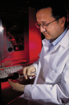
PHOTO CAPTION: A publication-quality photograph is available at ftp://ftp.purdue.edu/pub/uns/datta.nanotech.jpeg.
PHOTO CAPTION TWO: A publication-quality photograph is available at ftp://ftp.purdue.edu/pub/uns/datta.nanotech2.jpeg.
|

