
Innovation is step toward digital graphene transistors
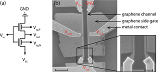
Researchers are making progress in creating digital transistors using a material called graphene, potentially sidestepping an obstacle thought to dramatically limit the material's use in computers and consumer electronics. This composite image shows the circuit schematics of a new type of graphene inverter, a critical building block of digital transistors, left, and scanning electron microscope images of the fabricated device. (Hong-Yan Chen, Purdue University Birck Nanotechnology Center)
WEST LAFAYETTE, Ind. - Researchers are making progress in creating digital transistors using a material called graphene, potentially sidestepping an obstacle thought to dramatically limit the material's use in computers and consumer electronics.
Graphene is a one-atom-thick layer of carbon that conducts electricity with little resistance or heat generation. After its discovery in 2004 - which earned a Nobel Prize in physics - it was touted as a potential replacement for silicon, possibly leading to ultrafast devices with simplified circuits that might be less expensive to manufacture.
However, graphene's luster has dulled in recent years for digital applications as researchers have discovered that it has no "band gap," a trait that is needed to switch on and off, which is critical for digital transistors.
"The fact that graphene is a zero-band-gap material by nature has raised many questions in terms of its usefulness for digital applications," said Purdue doctoral student Hong-Yan Chen.
Electrons in semiconductors like silicon exist at two energy levels, known as the valence and conduction bands. The energy gap between these two levels is called the band gap. Having the proper band gap enables transistors to turn on and off, which allows digital circuits to store information in binary code consisting of sequences of ones and zeroes.
Chen has led a team of researchers in creating a new type of graphene inverter, a critical building block of digital transistors. Other researchers have created graphene inverters, but they had to be operated at 77 degrees Kelvin, which is minus 196 Celsius (minus 320 Fahrenheit).
"If graphene could be used in digital applications, that would be really important," said Chen, who is working with Joerg Appenzeller, a professor of electrical and computer engineering and scientific director of nanoelectronics at Purdue's Birck Nanotechnology Center.
The Purdue researchers are the first to create graphene inverters that work at room temperature and have a gain larger than one, a basic requirement for digital electronics that enables transistors to amplify signals and control its switching from 0 to 1.
Findings were detailed in a paper, "Complementary-Type Graphene Inverters Operating at Room-Temperature," presented in June during the 2011 Device Research Conference in Santa Barbara, Calif.
Thus far graphene transistors have been practical only for specialized applications, such as amplifiers for cell phones and military systems. However, the new inverters represent a step toward learning how to use the material to create graphene transistors for broader digital applications that include computers and consumer electronics.
To create electronic devices, silicon is impregnated with impurities to change its semiconducting properties. Such "doping" is not easily applicable to graphene. However, the researchers have potentially solved this problem by developing "electrostatic doping," which makes it possible for graphene inverters to mimic the characteristics of silicon inverters.
Electrostatic doping is induced through the electric field between metal gates, which are located 40 nanometers away from graphene channels. The doping can be altered by varying the voltage, enabling researchers to test specific doping levels.
"This will allow us to find the sweet spot for operating the device," Chen said.
Further work will be needed to integrate the prototype into a working graphene circuit for digital applications.
The research is based at the Birck Nanotechnology Center in Purdue's Discovery Park.
Writer: Emil Venere, 765-494-4709, venere@purdue.edu
Sources: Joerg Appenzeller, 765-494-1076, appenzeller@purdue.edu
Hong-Yan Chen, chen200@purdue.edu
ABSTRACT
Complementary-Type Graphene Inverters Operating at Room Temperature
Hong-Yan Chen, Joerg Appenzeller
ECE Department and Birck Nanotechnology Center, Purdue University
Graphene has recently emerged as a promising candidate for a number of electronic applications. However, the fact that graphene is a zero-band-gap material by nature has raised many questions in terms of graphene's usefulness for digital applications. Several recent experimental studies have demonstrated graphene-based inverters, but issues remain, such as low inverter gain (0.044[1], 0.02[2]) and mismatch between input/output voltage levels [1,2]. Li et al. [3,4] reported top-gated complementary-like graphene inverters exhibiting a gain larger than 1. However, all data were obtained at 77K, and the implementation of a p-type and n-type FET was accomplished by relying on the intrinsic dependence of graphene's transfer characteristics on the supply voltage, an effect that is hardly controllable and that poses major problems for further device optimization. In this paper, focusing on inverter characteristics without attempting to build a highly scaled device, we report the first room-temperature, electrostatic-doping-controlled, complementary graphene inverter with a gain larger than one.