
New materials may bring advanced optical technologies, cloaking
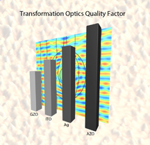
Researchers are developing a new class of "plasmonic metamaterials" as potential building blocks for advanced optical technologies and a range of potential breakthroughs in the field of transformation optics. This image shows the transformation optics "quality factor" for several plasmonic materials. For transformation optical devices, the quality factor rises as the amount of light "lost," or absorbed, by plasmonic materials falls, resulting in materials that are promising for a range of advanced technologies. (Birck Nanotechnology Center, Purdue University)
WEST LAFAYETTE, Ind. - Researchers are developing a new class of "plasmonic metamaterials" as potential building blocks for advanced optical technologies, including ultrapowerful microscopes and computers, improved solar cells, and a possible invisibility cloak.
The new materials could make possible "nanophotonic" devices for numerous applications, said Alexandra Boltasseva, an assistant professor of electrical and computer engineering at Purdue University.
Unlike natural materials, metamaterials may possess an index of refraction less than one or less than zero. Refraction occurs as electromagnetic waves, including light, bend when passing from one material into another. It causes the bent-stick-in-water effect, which occurs when a stick placed in a glass of water appears crooked when viewed from the outside.
Being able to create materials with an index of refraction that's negative or between one and zero promises a range of potential breakthroughs in a new field called transformation optics. However, development of new technologies using metamaterials has been hindered by two major limitations: too much light is "lost," or absorbed by metals such as silver and gold contained in the metamaterials, and the materials need to be more precisely tuned so that they possess the proper index of refraction.
Now, researchers are proposing a new approach to overcome these obstacles. Findings will be detailed in an article appearing Friday (Jan. 21) in the journal Science. The article was written by Boltasseva and Harry Atwater, Howard Hughes Professor and a professor of applied physics and materials science at the California Institute of Technology.
The researchers are working to replace silver and gold in materials that are created using two options: making semiconductors more metallic by adding metal impurities to them; or adding non-metallic elements to metals, in effect making them less metallic. Examples of these materials include aluminum oxides and titanium nitride, which looks like gold and is used to coat the domes of Russian churches.
Researchers have tested some of the new materials, demonstrating their optical properties and finding that they outperform silver and gold, in work based at the Birck Nanotechnology Center in Purdue's Discovery Park.
Plasmonic metamaterials are promising for various advances, including a possible "hyperlens" that could make optical microscopes 10 times more powerful and able to see objects as small as DNA; advanced sensors; new types of light-harvesting systems for more efficient solar cells; computers and consumer electronics that use light instead of electronic signals to process information; and a cloak of invisibility.
Optical nanophotonic circuits might harness clouds of electrons called "surface plasmons" to manipulate and control the routing of light in devices too tiny for conventional lasers.
Some of the new materials are showing promise in uses involving near-infrared light, the range of the spectrum critical for telecommunications and fiberoptics. Other materials also might work for light in the visible range of the spectrum. The new materials might be tuned so that their refractive index is ideal for specific ranges of the spectrum, allowing their use for particular applications.
Future photonics technologies will revolve around new types of optical transistors, switches and data processors. Conventional computers transmit and process pieces of information in serial form, or one piece at a time. However, future computers may use parallel streams of data, resulting in much faster networks and computers.
The work has been funded by the U.S. Army Research Office.
Writer: Emil Venere, 765-494-4709, venere@purdue.edu
Source: Alexandra Boltasseva, 765-494-0301, aeb@purdue.edu
Note to Journalists: Journalists may obtain a copy of the article by contacting the Science Press Package team at 202-326-6440, scipak@aaas.org
ABSTRACT
Low-Loss Plasmonic Metamaterials
Alexandra Boltasseva1, Harry Atwater2
1School of Electrical and Computer Engineering
and Birck Nanotechnology Center
Purdue University
2Applied Physics and Kavli Nanoscience Institute
California Institute of Technology
New materials are being developed that meet the requirements for nanoscale photonics. Metamaterials (MMs) are artificial, engineered materials with rationally designed compositions and arrangements of nanostructured building blocks. These materials can be tailored for almost any application because of their extraordinary response to electromagnetic, acoustic, and thermal waves that transcends the properties of natural materials. The astonishing MM?based designs and demonstrations range from a negative index of refraction, focusing and imaging with subwavelength resolution, invisibility cloaks, and optical black holes to nanoscale optics, data processing, and quantum information applications. Plasmonic MMs also face the challenge associated with overcoming the losses that dampen these subwavelength coupled excitations. One solution would be to combine MMs with a gain medium to offset the metallic losses. However, even the most active gain materials cannot fully compensate the large losses. A different approach would be the discovery of better plasmonic materials that have a negative real part of dielectric permittivity. This search requires an investigation of previously overlooked elements, improving the optical properties of the existing metallic materials via doping, or alloying and careful band?structure engineering.