Research
Research » 2D Materials » Schottky-barrier Injection
In order to utilize emerging 2D materials in electronic devices, it's essential to make good electrical contacts to the materials. Moreover, when extracting the properties of materials such as mobility, we need to understand the effects of contacts to separate them from the intrinsic properties.
Through analysis of experimental results, we found for many 2D materials of interest, such as transition metal dichacolgenides (TMDs) and black phosphorus, that the metal-to-semiconductor contacts are Schottky-barrier type. The following summarizes some highlights on Schottky-barrier devices.
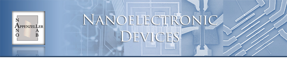
MoS2 Schottky-barrier Transistor with Scandium Contact
We present a thorough experimental study of contacts to MoS2 using low work function metals like scandium (ΦM = 3.5 eV) and titanium (ΦM = 4.3 eV) as well as large work function metals like nickel (ΦM = 5.0 eV) and platinum (ΦM = 5.9 eV) to shine some light on the impact of Schottky barriers on the carrier transport in MoS2 FETs. From a detailed temperature-dependent study that considers both thermionic emissions over the Schottky barrier as well as thermally assisted tunneling through the same, we have extracted the Schottky barrier height for the various metal electrodes and found ∼230 meV for platinum, ∼150 meV for nickel, ∼50 meV for titanium, and ∼30 meV for scandium. Our experiments provide unambiguous evidence that the MoS2-to-metal interface is strongly impacted by Fermi level pinning close to the conduction band of the MoS2, similar to the case of many III−V materials and silicon.
We demonstrate that through a proper understanding and design of source/drain contacts and the right choice of number of MoS2 layers the excellent intrinsic properties of this 2-D material can be harvested. Using scandium contacts on 10-nm-thick exfoliated MoS2 flakes that are covered by a 15 nm Al2O3 film, high effective mobilities of 700 cm2/(V·s) are achieved at room temperature. This breakthrough is largely attributed to the fact that we succeeded in eliminating contact resistance effects that limited the device performance in the past unrecognized (see Nano Letters, 2013, 13, 100-105).
Authors: Saptarshi Das, Ashish Penumatcha
Pictures adapted with permission from Nano Lett., 2013, 13, pp 100–105. Copyright © 2012 American Chemical Society.
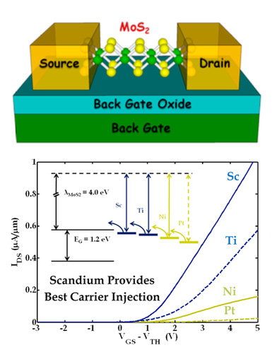
Tunability of short-channel effects in MoS2 Schottky-barrier Transistors
MoS2 transistors have been electrically characterized and analyzed in terms of their vulnerability to short channel effects and their response to various environments. We find that the electrical performance of MoS2 flakes is governed by an unexpected dependence on the effective body thickness of the device which in turn depends on the amount of intercalated water molecules that exist in the layered structure. In particular, we observe that the doping stage of a MoS2 field-effect transistor (FET) strongly depends on the environment (air/vacuum). Most importantly, our results indicate that device characteristics of MoS2 can be substantially impacted by tuning the device electrostatics. This can be accomplished by controlling the effectively active body thickness of the MoS2 FET employing intercalation and engineering of the effective barrier between individual MoS2 layers (see Nano Letters 15, 301-306 ).
Author: Feng Zhang
Pictures and abstract adapted with permission from Nano Letters 15, 301-306. Copyright © 2014 American Chemical Society.
Black Phosphorus Schottky-barrier MOSFET and Modeling
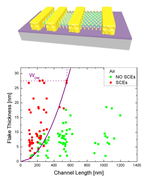
Black phosphorus(BP) is a newly rediscoverd layered 2D material. Each monolayer is comprised of phosphorus atoms arranged in a puckered fashion. Multiple monolayers are held together by weak Van der Waal’s forces. BP has a very high mobility (200-1000 cm2/V-s) and a direct bandgap. This makes it attractive for RF applications and also opto-electronics applications due to its tunable bandgap. Efforts are also on building tunnel FETs using BP.
Before, we begin to use 2D-materials to build devices it is extremely important that we study their material properties. One critical aspect of 2D-materials is the metal-semiconductor interface. BP transistors, like TMD transistors are Schottky barrier MOSFETs. A Schottky-barrier MOSFET (SB-MOSFET) can be thought of as two back-to-back Schottky diodes with the gate terminal controlling the entire channel from source to drain. In the off-state of the device, when the charge in the channel is negligible and the transmission through the device is limited by the Schottky barriers at the source and drain, the transfer characteristic can be quantitatively described using a simple Landauer model. By fitting the measured transfer characteristics using this model, a wealth of information can be extracted about the metal-semiconductor interface. We used this model to extract both electron- and hole-Schottky barrier heights of Permalloy and Palladium to black phosphorus. This model can be extended to other 2D-material SB-MOSFETs (see Nature Communications 6, 6:8948-1 – 6:8948-8).
Authors: Ashish Penumatcha, Ramon Salazar