
August 1, 2006
Purdue engineers lay groundwork for 'vertically oriented nanoelectronics'
WEST LAFAYETTE, Ind. — Engineers at Purdue University have developed a technique to grow individual carbon nanotubes vertically on top of a silicon wafer, a step toward making advanced electronics, wireless devices and sensors using nanotubes by stacking circuits and components in layers.
|
"Verticality gives you the ability to fit more things into the same area, so you can add more and more layers while keeping the footprint the same size or smaller," Fisher said. "But before we can even think about using nanotubes in electronics, we have to learn how to put them where we want them."
|
A mixture of hydrogen and methane gas was then flowed into the template's holes, and microwave energy was applied to break down the methane, which contains carbon. The iron layer acted as a catalyst that prompted the carbon nanotubes to assemble from carbon originating in the methane, and the tubes then grew vertically out of the cavities.
"You get a single nanotube in each pore, and that's important because we can start to think about controlling how and where to put nanotubes to vertically integrate them for future electronic devices and sensing technologies," Sands said.
Findings are detailed in a research paper that appeared July 11 in the journal Nanotechnology. The paper was written by graduate students Matthew R. Maschmann and Aaron D. Franklin; postdoctoral research associate Placidus Amama; Dmitri Zakharov, a staff scientist at Purdue's Birck Nanotechnology Center; Eric Stach, an associate professor of materials engineering; Sands and Fisher.
"The pores in the template and the nanotubes that grow in the pores really self-assemble once you set the process in motion," said Stach, who used two types of electron microscopes to take images of the nanotubes emerging vertically from the cavities. The research is based at the Birck Nanotechnology Center in Purdue's Discovery Park, the university's hub for interdisciplinary research.
The cavities form within seconds, and the nanotubes take several minutes to finish growing. The holes vary in width from 30-50 nanometers. A nanometer, or billionth of a meter, is about as long as 10 atoms strung together.
Carbon nanotubes, which were discovered in the early 1990s, might enable industry to create new types of transistors and more powerful, energy-efficient computers, as well as ultra-thin "nanowires" for electronic circuits. Reaching that potential promise, however, won't be possible unless carbon nanotubes can be integrated with other parts of circuitry and devices, Sands said.
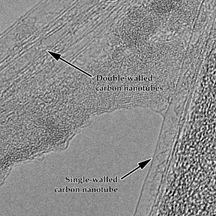
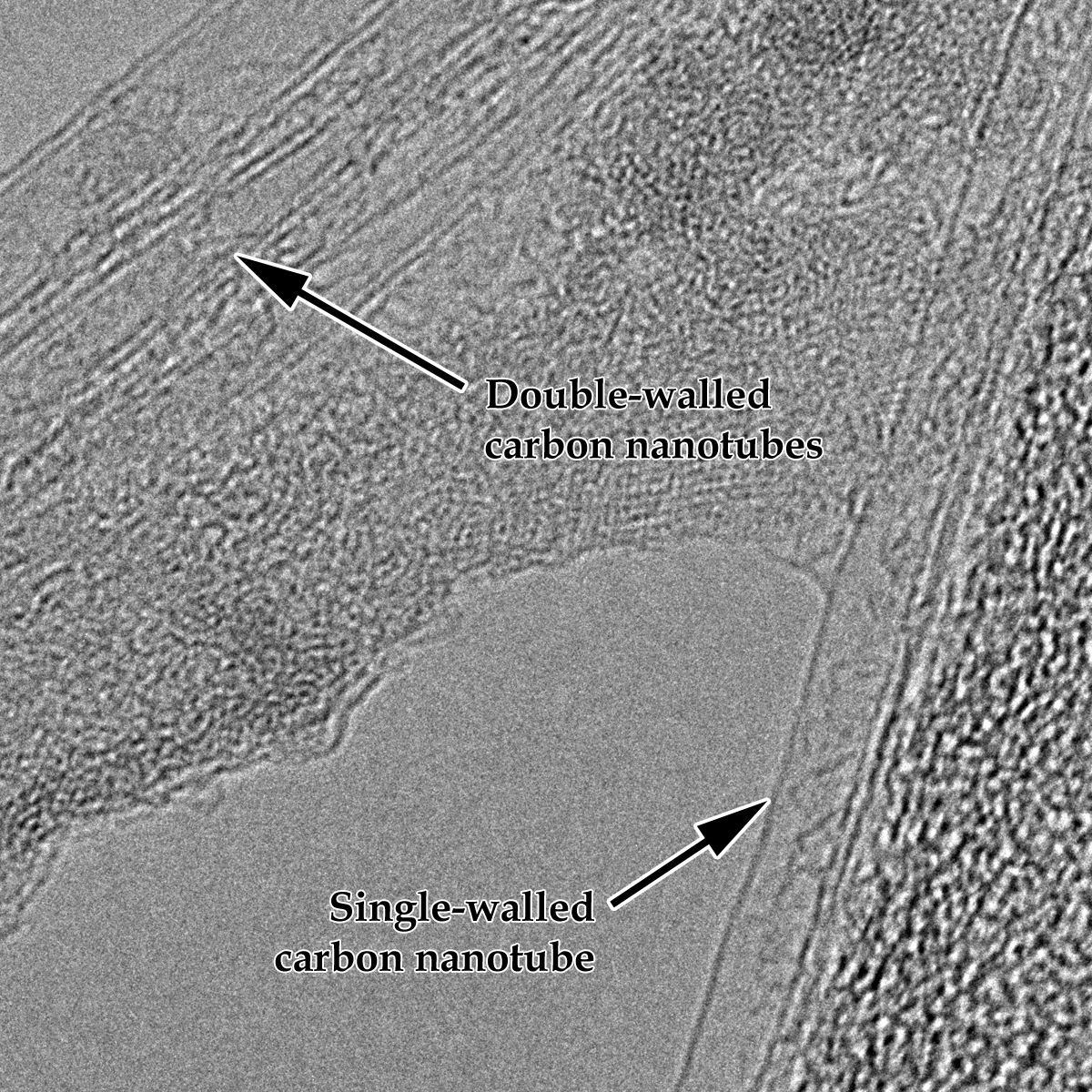
The experiments at Purdue yielded both single- and double-walled nanotubes, meaning they are made of either one or two single sheets of carbon atoms, yielding tubes about one nanometer in diameter.
Researchers will continue the work in efforts to understand which conditions are needed to produce single-wall tubes versus the double-wall variety and to learn how to produce more of one or the other.
Other researchers previously have made the templates, but the Purdue researchers are the first to add a layer of iron, which was Maschmann's idea, Fisher said.
"He was told by many people, including me, that it probably wouldn't work," Fisher said. "We were surprised to see that the nanotubes grow from the sidewall of the hole and then extend vertically."
Early applications are most likely in wireless computer networks and radar technology. Long-term uses are possible in new types of transistors, other electronic devices and circuits.
The research is funded by NASA, through the Purdue-based Institute for Nanoelectronics and Computing.
Writer: Emil Venere, (765) 494-4709, venere@purdue.edu
Sources: Timothy Fisher, (765) 494-5627, tsfisher@purdue.edu
Eric Stach, (765) 494-1466, eastach@purdue.edu
Timothy Sands, (765) 496-6105, tsands@ecn.purdue.edu
Matthew Maschmann, maschmann@purdue.edu
Purdue News Service: (765) 494-2096; purduenews@purdue.edu
Note to Journalists: An electronic copy of the research paper is available from Emil Venere, (765) 494-4709, venere@purdue.edu.
IMAGE CAPTION:
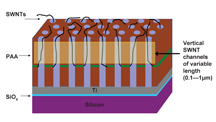
This diagram shows the "porous anodic alumina template" created by Purdue engineers to grow carbon nanotubes vertically out of tiny cavities on top of a silicon wafer. The technique might form a foundation for creating future "vertically oriented" nanoelectronic devices that can pack more devices and circuits into a computer chip while keeping the same footprint size as conventional chips. (Birck Nanotechnology Center, Purdue University)
A publication-quality photo is available at https://www.purdue.edu/uns/images/+2006/fisher-nano.jpg
PHOTO CAPTION:
This picture, taken with a transmission electron microscope, shows carbon nanotubes that have been grown out of tiny cavities in a "porous anodic alumina template" created by Purdue engineers. A layer of iron in the template acts as a catalyst to grow the nanotubes from methane gas flowed into the template. The technique might help develop a method for creating future "vertically oriented" nanoelectronic devices that pack more devices and circuits into a computer chip while keeping the same-size footprint as a conventional chip. (Birck Nanotechnology Center, Purdue University)
A publication-quality photo is available at https://www.purdue.edu/uns/images/+2006/fisher-vertical.jpg
Vertical single- and double-walled carbon nanotubes
grown from modified porous anodic alumina templates
Placidus B Amama 1, Dmitri N Zakharov1, Eric A Stach 1,4,
Timothy D Sands 1,3,4 and Timothy S Fisher 1,2,5
2 School of Mechanical Engineering, Purdue University, West Lafayette, IN 47907, USA;
2 School of Mechanical Engineering, Purdue University, West Lafayette, IN 47907, USA;
4 School of Materials Engineering, Purdue University, West Lafayette, IN 47907, USA
Vertical single-walled and double-walled carbon nanotube (SWNT and DWNT) arrays have been grown using a catalyst embedded within the pore walls of a porous anodic alumina (PAA) template. The initial film structure consisted of a SiOx adhesion layer, a Ti layer, a bottom Al layer, a Fe layer, and a top Al layer deposited on a Si wafer. The Al and Fe layers were subsequently anodized to create a vertically oriented pore structure through the film stack. CNTs were synthesized from the catalyst layer by plasma-enhanced chemical vapor deposition (PECVD). The resulting structure is expected to form the basis for development of vertically oriented CNT-based electronics and sensors.
To the News Service home page